Verification device and method for verifying an electrical overvoltage between electrical conductors

a technology of electrical conductor and verification device, which is applied in the direction of resistance/reactance/impedence, dynamo-electric machine testing, instruments, etc., can solve the problems of total failure of the machine, damage to the insulation,

Active Publication Date: 2021-02-02
SIEMENS AG
View PDF15 Cites 0 Cited by
  • Summary
  • Abstract
  • Description
  • Claims
  • Application Information

AI Technical Summary

Benefits of technology

[0009]A verification device according to the invention enables the verification of an overvoltage in that the overvoltage changes the electrical resistance of a conductor track so that the overvoltage can be verified by measuring the electrical resistance. Herein, the invention utilizes the fact that the electrical resistance of a suitably embodied conductor track can be changed by a partial discharge. Accordingly, according to the invention, to verify an overvoltage, the overvoltage triggers a partial discharge that changes the electrical resistance of a conductor track in the verification device. In particular, the invention enables the detection of overvoltages at coil windings of an electrical machine without there being any need to switch off or open the machine. As a result, overvoltages which could result in damage to the insulation of the coil windings and ultimately to a total failure of the machine can be detected in good time during the operation of the machine.
[0011]According to another advantageous feature of the present invention, the one conductor track can, as an alternative, be electrically connected to one of the two electrical conductors. Thus, the conductor track of which the electrical resistance is measured and used to verify the overvoltage is connected to one of the electrical conductors between which an overvoltage is to be detected. As a result, the number of conductor tracks of the verification device can be reduced and the verification device can be executed in a more compact and less expensive manner.
[0012]According to another advantageous feature of the present invention, the conductor tracks can be made of composite material which includes a non-electrically conductive plastic matrix and a filler which is embedded in the plastic matrix and renders the composite material electrically conductive. Advantageously, the filler can include electrically conductive filler particles arranged to occupy lattice sites of a lattice formed by the plastic matrix with a probability that is greater than a percolation threshold above which the composite material is electrically conductive, the filler particles having an electrical conductivity which is reduced by a partial discharge acting on the filler particles. The filler contains, for example, n-conducting metal oxide, coated or uncoated mica, quartz powder, carbon black, graphite and / or metal. In particular, the filler can contain antinomy-doped tin dioxide and / or fluorine- or indium-doped tin dioxide. Advantageously, the plastic matrix can be made of a chemically crosslinked thermoset or a thermoplastic. Thus, conductor tracks can be realized that have an electrical resistance which is increased by partial discharges as a result of making the conductor tracks of a suitable filled embedded in a plastic matrix. For example, during their production, filler particles made of antimony-doped tin dioxide automatically form oxygen vacancies that act as charge-carrier donors and contribute to the good electrical conductivity of the filler. A partial discharge caused by overvoltage heats the filler locally and causes a local generation of ozone. The temperature rise and the resulting ozone result in the oxidation of surface barrier layers of the filler particles with oxygen vacancies. This reduces the number of oxygen vacancies in the filler and the electrical conductivity of the composite material is reduced or the electrical resistance of the composite material is increased. The same applies to other fillers made of an n-conducting metal oxide that is suitably doped to improve its electrical conductivity, for example with a chemical element with an atomic number in the periodic table of elements that is one higher than the atomic number of the metal of the metal oxide. Filler particles made of carbon black, graphite or metal do not form surface barrier layers of the type described above with partial discharges, but oxidize in the case of partial discharges and thereby lose their electrical conductivity so that the electrical resistance of the composite material also increases in this case.
[0015]According to another advantageous feature of the present invention, the conductor-track carrier can be a plate or film. As a result, the verification device can easily and flexibly be used and assembled.
[0016]According to another advantageous feature of the present invention, at least one of the two electrical conductors can be electrically connected to several of the plurality of the conductor tracks, the conductor tracks being configured such that different prespecified overvoltages between the electrical conductors cause partial discharges between the one conductor track and different ones of the conductor tracks that are electrically connected to one of the two electrical conductors. In this way, the verification device can be used to verify different overvoltages.

Problems solved by technology

As a result, overvoltages which could result in damage to the insulation of the coil windings and ultimately to a total failure of the machine can be detected in good time during the operation of the machine.

Method used


Image

  • Verification device and method for verifying an electrical overvoltage between electrical conductors
  • Verification device and method for verifying an electrical overvoltage between electrical conductors

Examples


Embodiment Construction

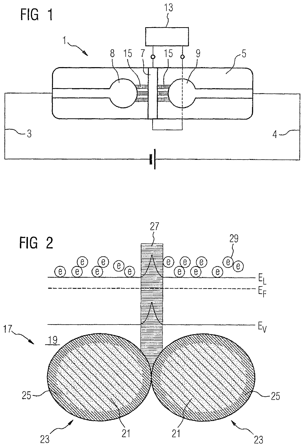
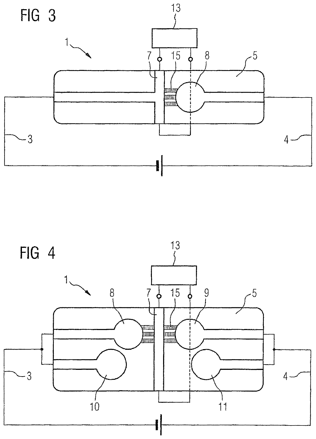
[0027]Throughout all the figures, same or corresponding elements may generally be indicated by same reference numerals. These depicted embodiments are to be understood as illustrative of the invention and not as limiting in any way. It should also be understood that the figures are not necessarily to scale and that the embodiments may be illustrated by graphic symbols, phantom lines, diagrammatic representations and fragmentary views. In certain instances, details which are not necessary for an understanding of the present invention or which render other details difficult to perceive may have been omitted.

[0028]Turning now to the drawing, and in particular to FIG. 1, there is shown a schematic illustration of a first exemplary embodiment of a verification device according to the present invention, generally designated by reference numeral 1, for verifying an electrical overvoltage between two electrical conductors 3, 4. The verification device 1 includes a conductor-track carrier 5,...


PUM


Abstract

A verification device for verifying an electrical overvoltage between two electrical conductors includes a conductor-track carrier made of an electrically insulating carrier material, a plurality of conductor tracks applied in spaced-apart relation from one another on the conductor-track carrier, and a measuring device acquiring an electrical resistance of one of the conductor tracks. Each of the two electrical conductors is electrically connected to at least one of the conductor tracks with the proviso that none of the conductor tracks is electrically connected to both of the two electrical conductors. The conductor tracks are configured such that a prespecified overvoltage between the two electrical conductors causes a partial discharge that changes the electrical resistance of the one conductor track between the one conductor track and another one of the conductor tracks that is electrically connected to one of the two electrical conductors.

Description

CROSS-REFERENCES TO RELATED APPLICATIONS[0001]This application claims the priority of European Patent Application, Serial No. 17211117.1, filed Dec. 29, 2018, pursuant to 35 U.S.C. 119(a)-(d), the disclosure of which is incorporated herein by reference in its entirety as if fully set forth herein.BACKGROUND OF THE INVENTION[0002]The present invention relates to a verification device and a method for verifying an electrical overvoltage between two electrical conductors.[0003]The following discussion of related art is provided to assist the reader in understanding the advantages of the invention, and is not to be construed as an admission that this related art is prior art to this invention.[0004]Overvoltages between insulated electrical conductors can in particular impair the insulation of the conductors. Insulation typically has production-related defects in the form of pores and gaps with expansions in the micrometer to millimeter range. Overvoltages can cause partial discharges in...

Claims


Application Information

Patent Timeline
Patent Type & Authority Patents(United States)
IPC IPC(8): G01R31/34G01R31/12G01R27/00
CPCG01R31/343G01R27/00G01R31/1272G01R31/346G01R19/165G01R31/1263G01R31/12H02H3/22
Inventor HELLER, JANISKATZENBERGER, TOBIASPLOCHMANN, BASTIAN
Owner SIEMENS AG
Why Eureka
Try Eureka