Insulation systems and methods of depositing insulation systems

a technology of insulation systems and depositing systems, applied in the direction of dielectric characteristics, semiconductor/solid-state device details, association of printed circuit non-printed electric components, etc., can solve the problems of converter reliability, the effect of reducing the insulation dramatically, and the potential has not yet been fully achieved

Active Publication Date: 2021-04-06
GENERAL ELECTRIC CO
View PDF15 Cites 0 Cited by
  • Summary
  • Abstract
  • Description
  • Claims
  • Application Information

AI Technical Summary

Problems solved by technology

However, this potential has not yet been fully attained due at least in part to capabilities of electrical insulation, particularly, in the packaging and connection for high voltage wide-bandgap devices.
The high electric fields that go with high voltage and high rate of change of voltage (e.g., greater than 10 kV per microsecond) lead to partial discharge within the insulation and creeping discharges on surfaces of semiconductor devices and busbars of the power converters, which may dramatically reduce the insulation, and hence converter, reliability.

Method used


Image

  • Insulation systems and methods of depositing insulation systems
  • Insulation systems and methods of depositing insulation systems
  • Insulation systems and methods of depositing insulation systems

Examples


Embodiment Construction

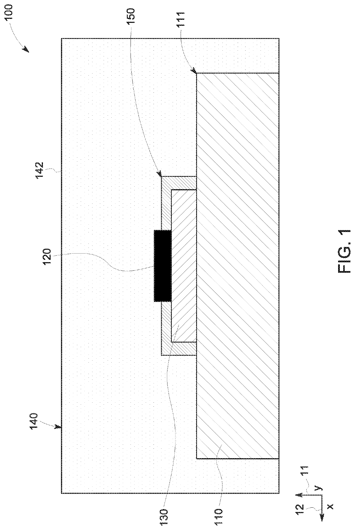
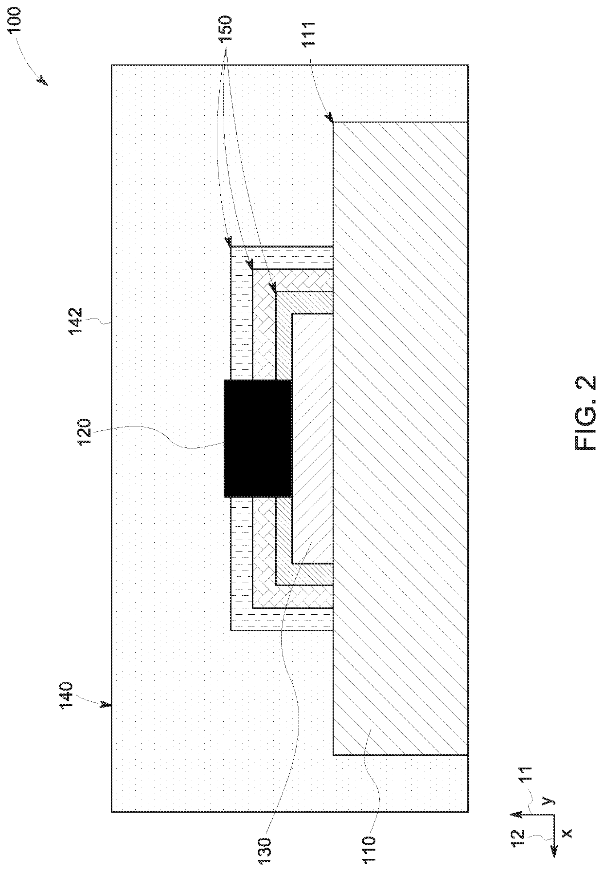
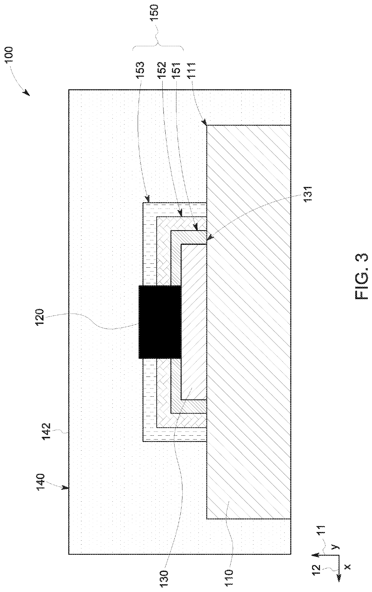
[0019]One or more specific embodiments of the present embodiments described herein will be described below. In an effort to provide a concise description of these embodiments, all features of an actual implementation may not be described in the specification. It should be appreciated that in the development of any such actual implementation, as in any engineering or design project, numerous implementation-specific decisions must be made to achieve the developers' specific goals, such as compliance with system-related and business-related constraints, which may vary from one implementation to another. Moreover, it should be appreciated that such a development effort might be complex and time consuming, but would nevertheless be a routine undertaking of design, fabrication, and manufacture for those of ordinary skill having the benefit of this disclosure.

[0020]When introducing elements of various embodiments of the present disclosure, the articles “a,”“an,” and “the” are intended to m...


PUM

PropertyMeasurementUnit
relative dielectric constantaaaaaaaaaa

Abstract

This present disclosure generally relates to systems and methods of electrophoretic deposition (EPD) techniques for use in insulation systems at least partially encapsulating a semiconductor device, a conductive component and a substrate, such as insulation systems of semiconductor devices, busbars, or the like. Insulation systems formed using EPD processes may be designed to have a dielectric constant that decreases in a direction away from a substrate of the insulation system. This may improve insulation technologies since depositing coatings with sequentially arranged dielectric constants may improve resistance of the insulation system to high temperature, high electric fields, or the like.

Description

TECHNICAL FIELD[0001]The subject matter disclosed herein relates to techniques for depositing insulation systems on semiconductor devices, busbars, and other suitable devices.BACKGROUND[0002]Embodiments of the disclosure generally relate to insulation systems for semiconductor devices and busbars. More particularly, embodiments of the disclosure relate to electrophoretic processes for depositing insulation systems on semiconductor devices and busbars.[0003]Power electronic converter technology, which uses semiconductor switches to achieve full control of terminal voltages and currents, has seen tremendous advancement in applications in various power systems. This has largely been driven by the increasing availability of higher power switching devices such as those based on the SiC and GaN wide-bandgap semiconductors. These may enable a high voltage (e.g. 20 kilovolts (kV)) and / or high power (e.g., greater than 100 kilowatts (kW)) density converter with a relatively smaller size than...

Claims


Application Information

Patent Timeline
Patent Type & Authority Patents(United States)
IPC IPC(8): C25D13/12H01L23/495H01L23/29H05K3/10H01L21/56H05K1/11H05K1/18
CPCC25D13/12H01L21/56H01L23/295H01L23/49586H05K1/119H05K1/185H05K3/10H05K2201/0104H05K2203/135H01L23/293H01L23/3121C25D13/02
Inventor YIN, WEIJUNDUGGAL, ANIL RAJRAJU, RAVISEKHAR NADIMPALLI
Owner GENERAL ELECTRIC CO
Why Eureka
Try Eureka