Method of forming a semiconductor memory device with a laterally etched bottom dielectric layer

a dielectric layer and semiconductor technology, applied in the direction of semiconductor devices, transistors, electrical devices, etc., can solve the problems of increasing the rc delay and many defects in the dram cell with the buried gate, and achieve the effect of increasing the exposed portion of the substra

Active Publication Date: 2021-04-06
UNITED MICROELECTRONICS CORP +1
View PDF13 Cites 0 Cited by
  • Summary
  • Abstract
  • Description
  • Claims
  • Application Information

AI Technical Summary

Benefits of technology

[0004]One object of the present invention is to provide a method of forming a semiconductor memory device, in which, a multilayer structure of a dielectric layer disposed below bit lines are patterned respectively during different processes, so that, only a bottom layer of the multilayer structure of the dielectric layer has a retracted sidewall, for exposing more portion of the substrate. That is, the method of the present invention enables to form preferably plug for providing better connection with the substrate, and to obtain a better semiconductor memory device thereby, for improving the electrical connection between the storage node and the transistor underneath.
[0005]One object of the present invention is to provide a semiconductor memory device, in which, only a bottom layer of a dielectric layer disposed below the bit lines has a retracted sidewall, for exposing more portion of the substrate. That is, the semiconductor memory device of the present application may obtain more contact area between the substrate and plugs formed subsequently, so as to gain a better structure for improving the electrical connection between the storage node and the transistor underneath.
[0008]In summary, the method of the present invention utilizes the forming process of the spacer structure to simultaneously pattern a portion of the dielectric material layer, to make partial layers of the multilayer structure of the dielectric material layer being vertical aligned with the sidewall of the spacer structure, followed by further patterned the rest bottom layer of the multilayer structure of the dielectric material layer while defining the plug trenches in the subsequent process. In this way, the dielectric layer formed thereby may obtain misaligned sidewalls in each layer, and only the oxide layer disposed at the bottom of the multilayer structure will be laterally etched to have a retracted sidewall without directly in contact with the spacer layer. That is, the semiconductor memory device obtained in the present invention may sufficiently increase the expose portion of the substrate without further affecting the depth or the shape of the plug trenches, and then, the plugs formed in those plug trenches may therefore obtain more contact areas with the substrate, so as to avoid the disconnection between the storage node contact and the transistor.

Problems solved by technology

However, due to limitations in fabrication technologies, many defects are formed in the DRAM cell with the buried gate.
Furthermore, the shrunk spaces between wires also increase the parasitic capacitance (C), so that, the RC delay is therefore increase to achieve poor efficiency.

Method used


Image

  • Method of forming a semiconductor memory device with a laterally etched bottom dielectric layer
  • Method of forming a semiconductor memory device with a laterally etched bottom dielectric layer
  • Method of forming a semiconductor memory device with a laterally etched bottom dielectric layer

Examples


Embodiment Construction

[0023]To provide a better understanding of the present invention, preferred embodiments will be described in detail. The preferred embodiments of the present invention are illustrated in the accompanying drawings with numbered elements.

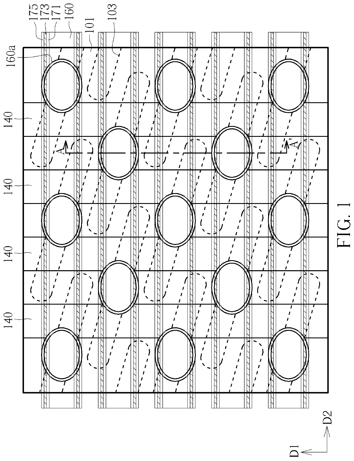
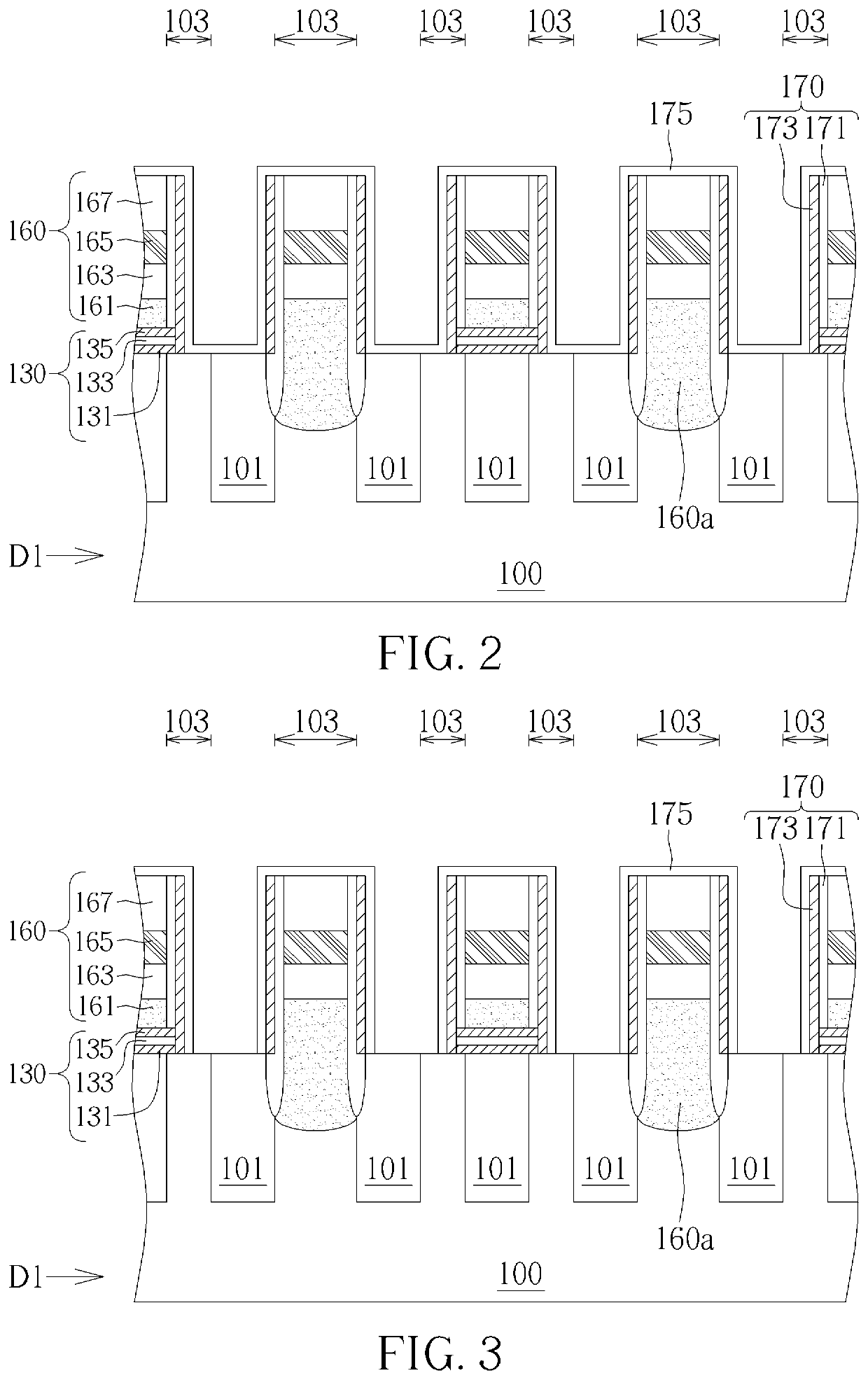
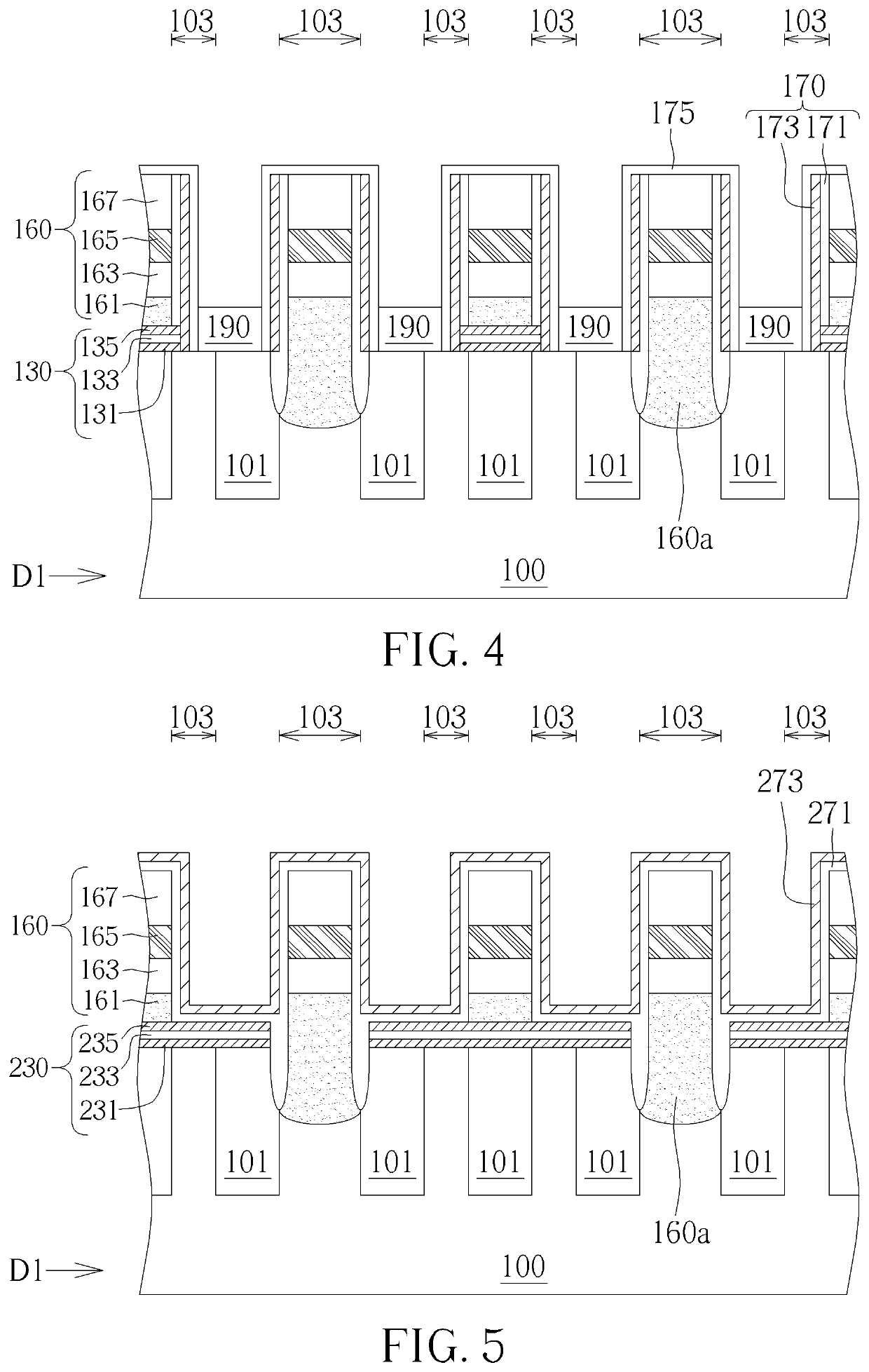
[0024]Referring to FIGS. 1-4, FIGS. 1-4 illustrate a forming method of semiconductor device according to the first preferred embodiment of the present invention, in which, FIG. 1 shows a top view of a semiconductor memory device during the forming method, and FIGS. 2-4 show a cross-sectional views of a semiconductor memory device during the forming method respectively. The semiconductor memory device of the present embodiment is for example a dynamic random access memory (DRAM) device which at least includes at least one transistor structure (not shown in the drawings) and at least one capacitor structure (not shown in the drawings), thereto serve as the smallest unit in the DRAM array for accepting signals from bit lines 160 and word lines 140 during...


PUM

PropertyMeasurementUnit
areaaaaaaaaaaa
sizeaaaaaaaaaa
channel lengthaaaaaaaaaa

Abstract

A semiconductor memory device and a method of forming the same, the semiconductor memory device includes a substrate, a dielectric layer, plural bit lines, at least one bit line contact, a spacer structure and a spacer layer. The substrate has an isolation area to define plural active areas. The dielectric layer is disposed on the substrate, and the dielectric layer includes a bottom layer having a sidewall being retracted from sidewalls of other layers of the dielectric layer. The plural bit lines are disposed on the dielectric stacked structure, along a direction, and the at least one bit line contact is disposed below one of the bit lines, within the substrate. The spacer structure is disposed at sidewalls of each of the bit lines, and the spacer layer is disposed on the spacer structure to directly in contact with the spacer structure and the other layers of the dielectric layer.

Description

BACKGROUND OF THE INVENTION1. Field of the Invention[0001]The present invention generally relates to the field of semiconductor memory devices and forming method thereof, and more particularly to a dynamic random access memory (DRAM) device and a forming method thereof.2. Description of the Prior Art[0002]For years the trend in the memory industry as well as the semiconductor industry has been to scale down the size of memory cells in order to increase the integration level and thus the memory capacity of DRAM chips. In a DRAM cell with a buried gate, the current leakage caused by a capacitor is often reduced or avoided thanks to a relatively long channel length beneath the buried gate. Therefore, more and more DRAM cells are equipped with buried gates rather than with a conventional planar gate structure due to their superior performances.[0003]In general, the DRAM cells with a buried gate include a transistor device and a charge storage device, which is able to accept signals from...

Claims


Application Information

Patent Timeline
Patent Type & Authority Patents(United States)
IPC IPC(8): H01L27/108
CPCH01L27/10823H01L27/10855H01L27/10876H01L27/10885H01L27/10888H01L21/76224H10B12/34H10B12/053H10B12/485H10B12/482H10B12/0335
Inventor LU, CHIEN-MINGLEE, FU-CHECHANG, FENG-YI
Owner UNITED MICROELECTRONICS CORP
Why Eureka
Try Eureka