Passive semiconductor device assembly technology

a semiconductor device and passive technology, applied in the field of passive semiconductor device assembly, can solve the problems of compromising the structural integrity of the device, the size of the device, and the difficulty of handling and packaging the device, and achieve the effect of increasing efficiency

Active Publication Date: 2021-04-20
NU NANO LTD
View PDF4 Cites 0 Cited by
  • Summary
  • Abstract
  • Description
  • Claims
  • Application Information

AI Technical Summary

Benefits of technology

[0010]Advantageously, the method and apparatus provided avoid the need to use post-assembly processes that can contaminate devices, whilst increasing the efficiency with which different processing requirements are distributed. Beneficially, the method and apparatus can be used in combination with a range of permanent bonding mechanisms to provide fully assembled devices. Furthermore, advantageously, the apparatus can be reused without any additional or repeat processing.

Problems solved by technology

Whilst it is known to decrease the size of devices in order to increase the number of devices produced from one wafer, the reduction in device size can compromise the structural integrity of the devices and lead to difficulties in handling and packaging the devices.
Consequently, the production of smaller devices may require more complex procedures to be implemented in order to deal with the smaller devices.
However, such machines are limited in the size of components that they can handle.
Whilst pick-and-place techniques are typically used to assemble semiconductor components ranging in size from a couple of hundred micrometres to several millimetres, for extremely small devices, pick-and-place cannot be used since the traditional vacuum tool cannot be machined with a sufficiently small enough aperture, e.g., less than 100 micrometres in diameter.
Therefore reduction of the size of device on a wafer is limited by the subsequent procedures that the device must be subjected to.
Furthermore, the size and shape of a device imposes limitations on the speed at which any tool handling the device can operate.
For example, very thin devices are more prone to breaking upon contact with a pick-and-place tool and devices only slightly larger than the pick-and-place tool are held less securely and are more likely to rotate or shear during assembly.
However, such adhesive material is necessarily removed before the device is operated.
Disadvantageously, this requires further processing steps in order to apply and remove the adhesive material, which increases processing time and increases the risk of contamination of the devices.

Method used


Image

  • Passive semiconductor device assembly technology
  • Passive semiconductor device assembly technology
  • Passive semiconductor device assembly technology

Examples


Embodiment Construction

[0012]Embodiments of the invention are now described, by way of example only, with reference to the accompanying drawings, in which:

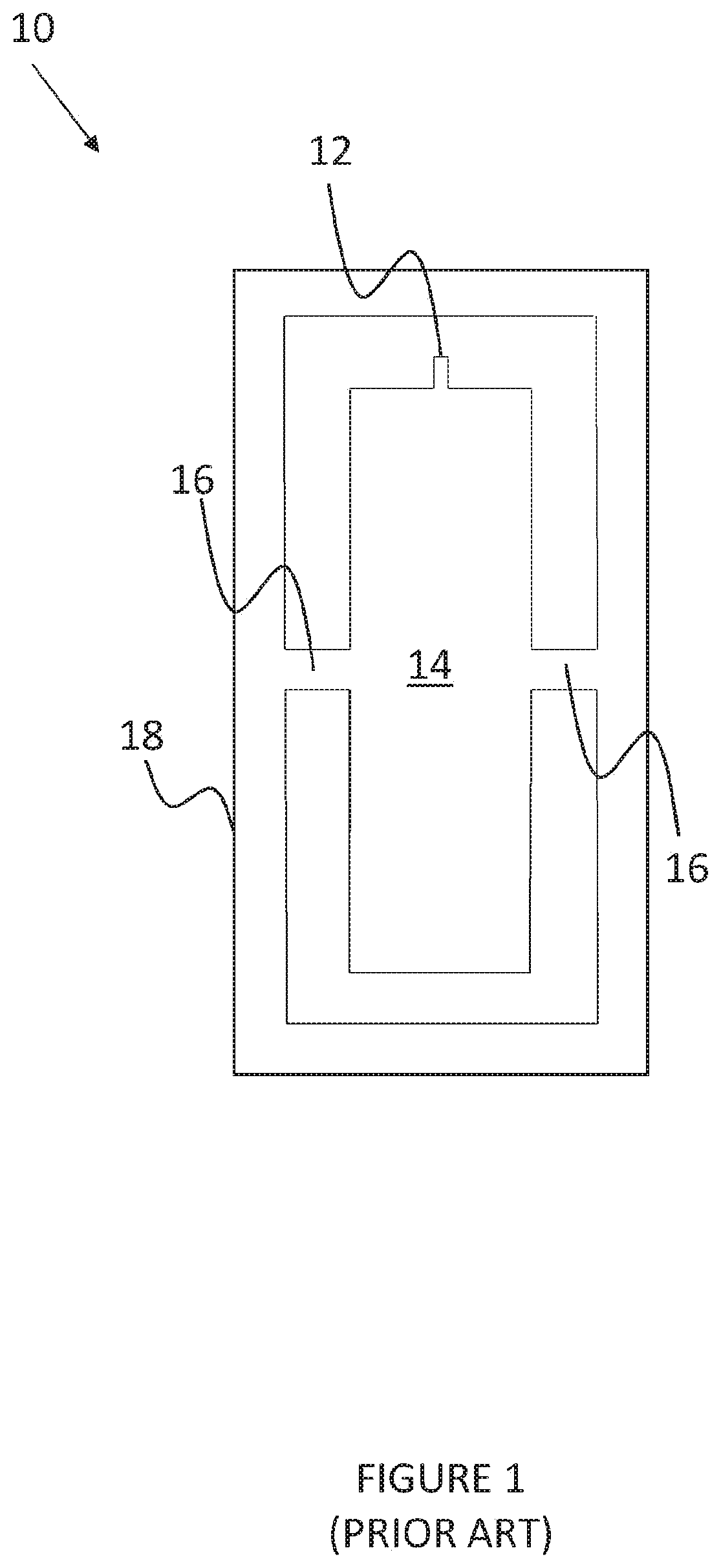
[0013]FIG. 1 is an example schematic of a prior art AFM probe;

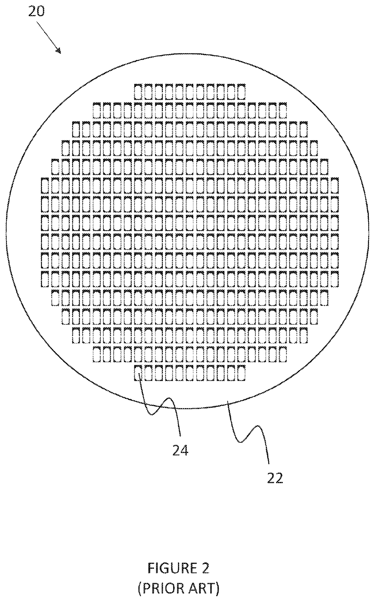
[0014]FIG. 2 is an example schematic of a processed prior art wafer containing AFM probes;

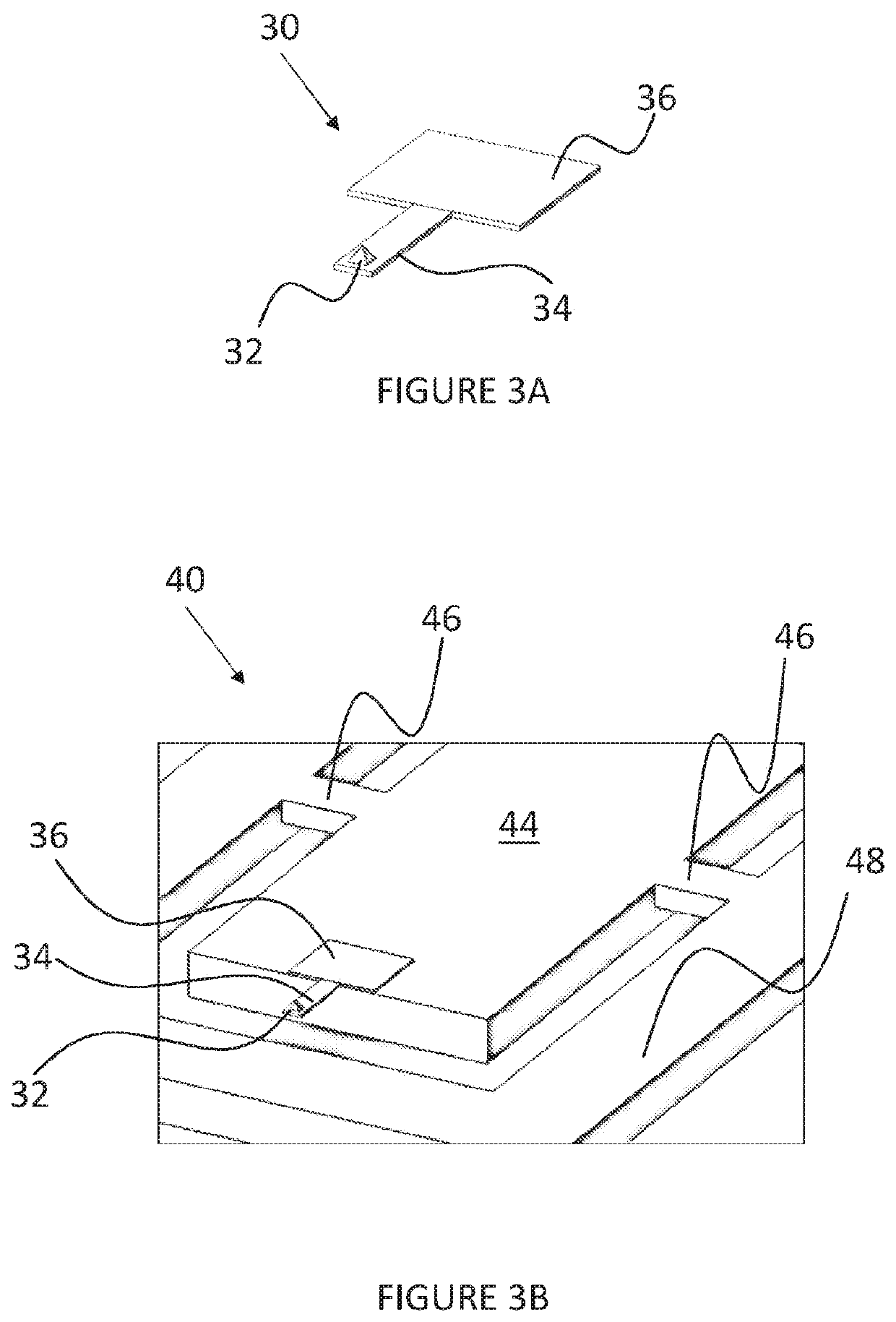
[0015]FIG. 3A is a perspective view of an AFM tip and cantilever construction;

[0016]FIG. 3B is a perspective view of an AFM probe in accordance with the invention;

[0017]FIG. 4 is a flow diagram of a method of assembling devices, in accordance with the invention;

[0018]FIG. 5A is a schematic of an array of AFM components;

[0019]FIG. 5B is a schematic of the array of AFM components of FIG. 5B with a group of components removed;

[0020]FIG. 6A is a schematic of the array of AFM components of FIG. 5A showing the relative position of a first group of components on a host device;

[0021]FIG. 6B is a schematic of the array of AFM components of FIG. 5B showing the relative position of a second group of components on a...


PUM

PropertyMeasurementUnit
diameteraaaaaaaaaa
sizeaaaaaaaaaa
thickaaaaaaaaaa

Abstract

A method of assembling a group of devices, the method comprising the steps of: evacuating a space between each component of a first group of two or more components on a source device and a transfer device thereby to create a temporary bond between each component of the first group of two or more components and the transfer device; selectively removing the first group of two or more components from the source device whilst the transfer device is temporarily bonded to each component of the first group of two or more components on the source device; positioning the first group of two or more components on a host device; and decoupling the first group of two or more components from the transfer device, thereby to form a first group of assembled devices.

Description

FIELD OF THE INVENTION[0001]The invention relates to apparatuses and methods for assembling devices. In particular, but not exclusively, the invention relates to the assembly of semiconductor devices, such as Atomic Force Microscopy (AFM) probes.BACKGROUND OF THE INVENTION[0002]Semiconductor devices and micro-fabricated devices, such micro-electromechanical systems (MEMS) and sensors are now ubiquitous in every day portable electronics. Current developments in this field, to drive greater uptake, include both the addition of functionality and the reduction of the size and cost of such devices.[0003]Semiconductor and micro-fabricated devices are typically produced by the mechanical and / or chemical processing of wafers. It is traditional semiconductor industry practice to simply shrink the size of devices in order to increase the density of devices on a wafer. The increased density of devices on a wafer maximises the use of wafer material and therefore the reduction in device size can...

Claims


Application Information

Patent Timeline
Patent Type & Authority Patents(United States)
IPC IPC(8): H01L21/50G01Q60/38G01Q60/28H01L21/68H01L21/683
CPCG01Q60/38G01Q60/28H01L21/50H01L21/681H01L21/6838G01Q70/02H01L21/6835B81C99/002
Inventor VICARY, JAMES
Owner NU NANO LTD
Why Eureka
Try Eureka