Eureka AIR delivers breakthrough ideas for toughest innovation challenges, trusted by R&D personnel around the world.

Method of forming split gate memory cells with thinned tunnel oxide

Active Publication Date: 2021-05-25
SILICON STORAGE TECHNOLOGY
View PDF12 Cites 3 Cited by
  • Summary
  • Abstract
  • Description
  • Claims
  • Application Information

AI Technical Summary

Benefits of technology

The present invention is a method for forming a memory device that has a logic region and a memory cell region in a semiconductor substrate. This method includes steps of forming a floating gate, an oxide layer, a non-conformal layer, a control gate, and a logic gate. The non-conformal layer is a protective layer that helps to prevent oxidation of the underlying layers during the process. The technical effect of this method is to improve the reliability and performance of the memory device.

Problems solved by technology

One drawback of the above described technique is that the thickness of oxide layer 26 must be compatible for both the logic devices and the memory cells.
Therefore, balancing these considerations, there is a lower limit to the thickness of oxide layer 26 driven by the high voltage operation of the logic device, which means the tunnel oxide in the memory cells is unnecessarily thick and therefore limits erase performance and efficiency, and limits endurance performance.
However, forming the tunneling oxide separately from the word line oxide and the logic gate oxide can significantly increase manufacturing complexity, time and costs.

Method used


Image

  • Method of forming split gate memory cells with thinned tunnel oxide
  • Method of forming split gate memory cells with thinned tunnel oxide
  • Method of forming split gate memory cells with thinned tunnel oxide

Examples


Embodiment Construction

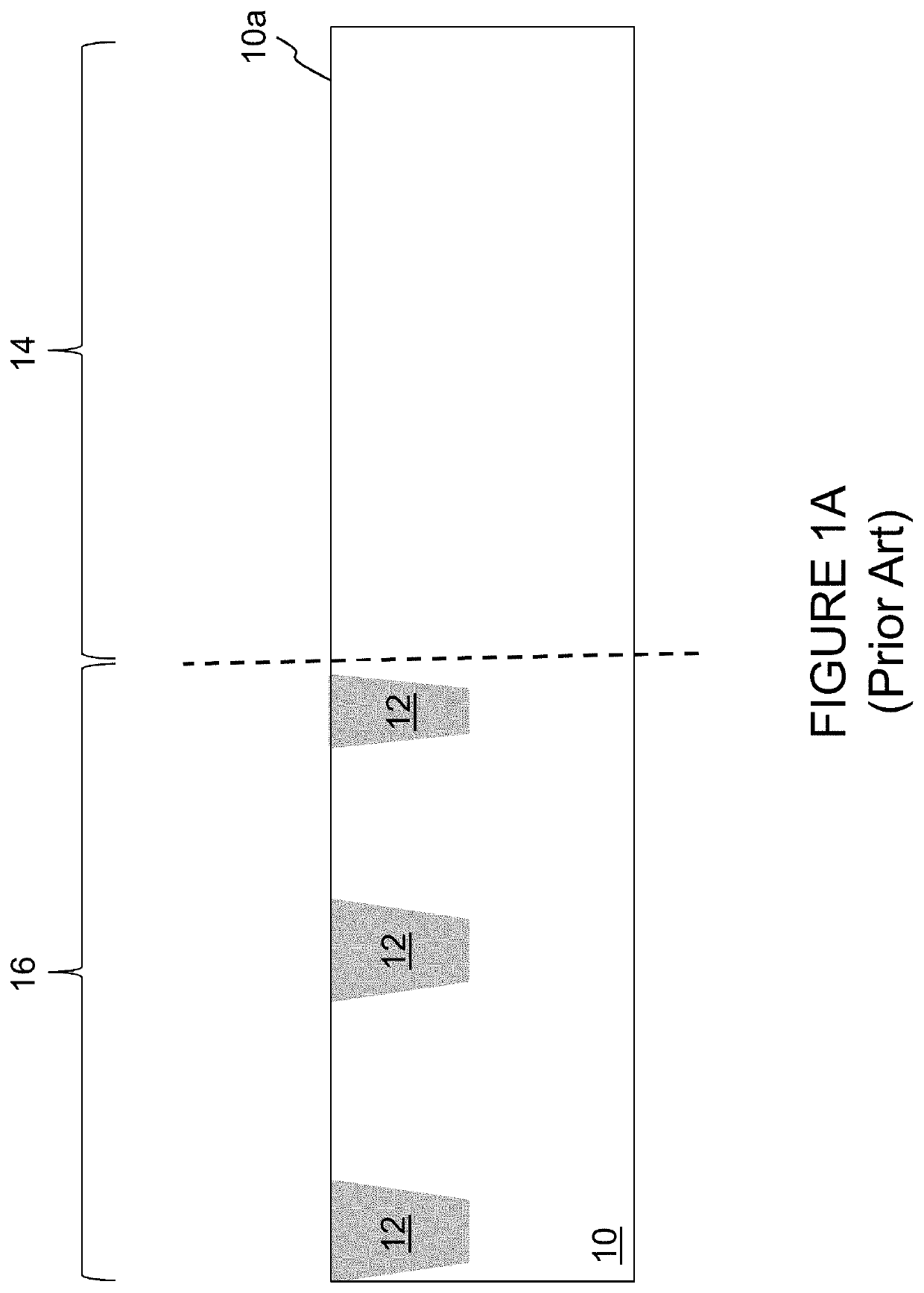
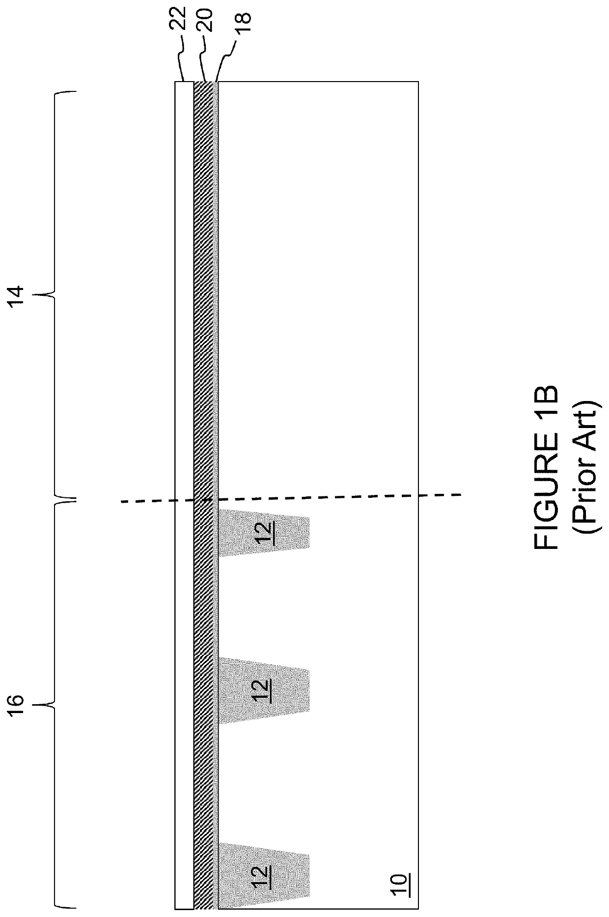
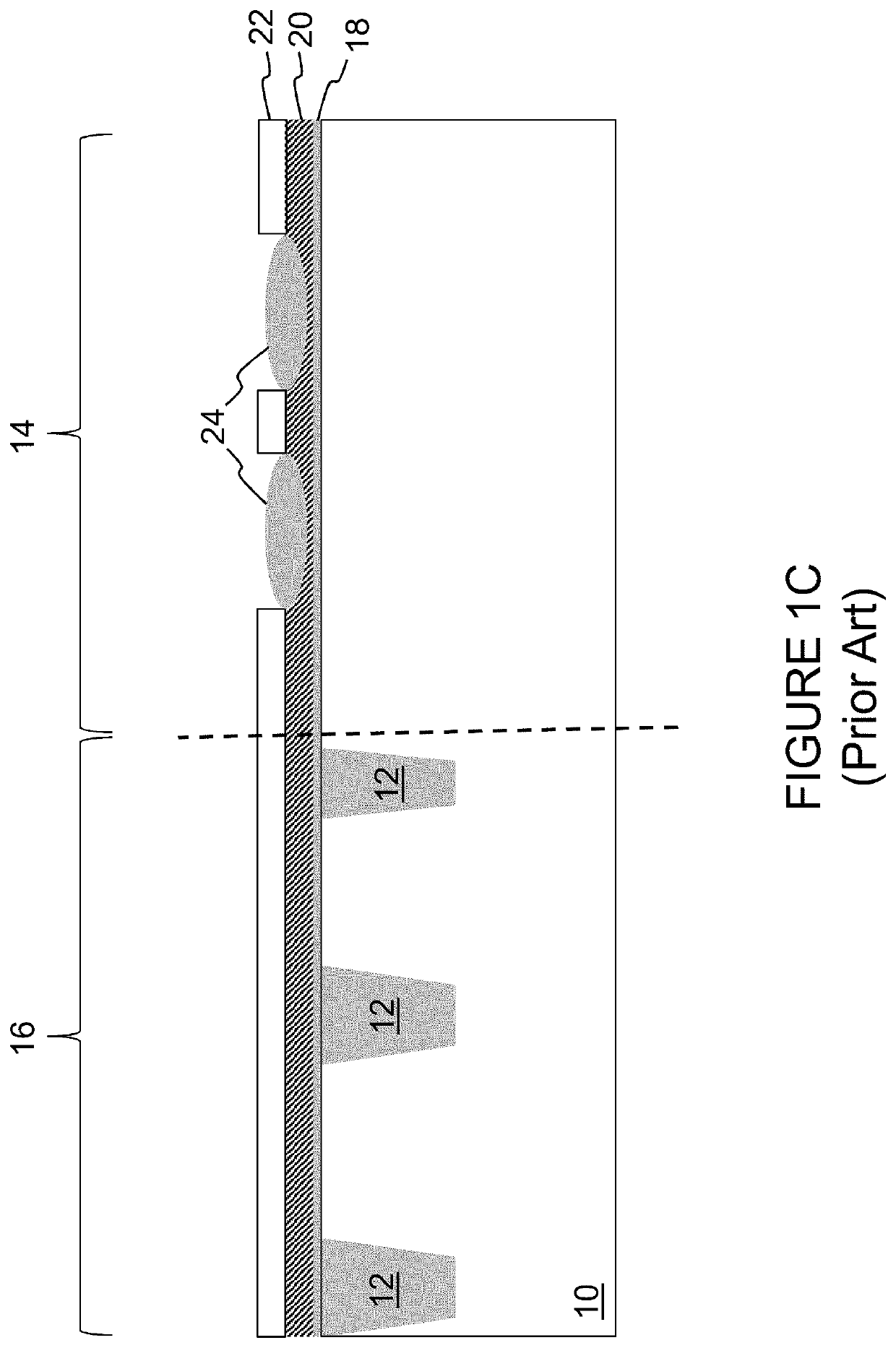
[0015]The present invention is a technique of forming memory cells and logic devices on a common substrate, where the oxide layer used as a tunnel oxide and word line oxide for the memory cells and the gate oxide for the logic devices is thinned in the memory cell region as it passes between the floating gate and the control gate.

[0016]FIGS. 2A-2F disclose the steps of the method of the present invention. The process begins using the same steps described above with respect to FIGS. 1A-1D. Starting with the structure in FIG. 1D, an oxide etch is used to remove the exposed portions of oxide layer 18 (i.e., those portions not under floating gate 20a. An oxide layer 26 is then formed over the structure either by deposition (which also thickens oxide areas 24) and / or by oxidation (which has no effect on oxide areas 24) as shown in FIG. 2A. Oxide layer 26 can be considered to have three portions: a first portion 26a that extends along the logic region of the substrate upper surface, a sec...


PUM


Abstract

A method of forming a memory device includes forming a floating gate on a memory cell area of a semiconductor substrate, having an upper surface terminating in an edge. An oxide layer is formed having first and second portions extending along the logic and memory cell regions of the substrate surface, respectively, and a third portion extending along the floating gate edge. A non-conformal layer is formed having a first, second and third portions covering the oxide layer first, second and third portions, respectively. An etch removes the non-conformal layer third portion, and thins but does not entirely remove the non-conformal layer first and second portions. An etch reduces the thickness of the oxide layer third portion. After removing the non-conformal layer first and second portions, a control gate is formed on the oxide layer second portion and a logic gate is formed on the oxide layer first portion.

Description

FIELD OF THE INVENTION[0001]The present invention relates to split-gate non-volatile memory cells, and more particularly to a method of forming such cells.BACKGROUND OF THE INVENTION[0002]Split-gate type memory cell arrays are known. For example, U.S. Pat. No. 5,029,130, which is incorporated herein by reference for all purposes, discloses a split gate memory cell and its formation, which includes forming source and drain regions in the substrate with a channel region there between. A floating gate is disposed over and controls the conductivity of one portion of the channel region, and a control gate is disposed over and controls the conductivity of the other portion of the channel region. The control gate extends up and over the floating gate. The insulation between the floating gate and the control gate is referred to as the tunnel dielectric material (e.g. oxide), because electrons tunnel through this dielectric material during the erase operation.[0003]It is also known to form h...

Claims


Application Information

Patent Timeline
IPC IPC(8): H01L21/00H01L27/11534H01L21/28H01L21/311H01L21/02H01L29/423H01L29/08H01L21/027H01L27/11521H01L29/788
CPCH01L27/11534H01L21/0223H01L21/0276H01L21/28079H01L21/31111H01L27/11521H01L29/0847H01L29/40111H01L29/42328H01L29/7883H01L29/40114H01L29/42324H10B41/44H10B41/43H10B41/30
Inventor KIM, JINHOCUEVAS, ELIZABETHGHAZAVI, PARVIZBERTELLO, BERNARDFESTES, GILLESDECOBERT, CATHERINETKACHEV, YURIVILLARD, BRUNODO, NHAN
Owner SILICON STORAGE TECHNOLOGY
Why Eureka
Eureka Blog
Learn More