Display device and method for manufacturing the same

a technology of display device and manufacturing method, which is applied in the field of display device, can solve the problems of low heat insufficient resistance of polarizing plate, and difficulty in forming electrode pattern directly on polarizing plate, and achieve the effect of high reliability of display devi

Active Publication Date: 2021-07-27
SEMICON ENERGY LAB CO LTD
View PDF88 Cites 6 Cited by
  • Summary
  • Abstract
  • Description
  • Claims
  • Application Information

AI Technical Summary

Benefits of technology

[0009]A structure in which an electrode of a touch sensor is provided between a polarizing plate and one of two substrates which interpose a display element is effective in reducing the thickness of a display device. However, a conventional method as described in Patent Document 1 has problems described below.

Problems solved by technology

However, a conventional method as described in Patent Document 1 has problems described below.
However, in general, a polarizing plate has low heat resistance and has insufficient resistance to a film formation step or an etching step of a conductive film, for example, and thus it is difficult to form a pattern of the electrode directly on the polarizing plate.
Further, a polarizing plate has insufficient resistance to heat or the like which is applied in a pressure bonding step of electrically connecting the electrode of the touch sensor and a flexible printed circuit (FPC) or the like, and thus it is difficult to connect an FPC or the like.
Therefore, it is extremely difficult to provide the electrode of the touch sensor on one surface of the polarizing plate.
However, in the case of forming a color filter or an electrode of a touch sensor on respective surfaces of a substrate in this manner, there is a problem in that the color filter is damaged by a member such as a stage of an apparatus being in contact with the surface where the color filter is formed, for example, at the time of forming a pattern of the electrode on the back surface of the substrate the front surface of which is provided with the color filter.
Further, also in the case where the electrode of the touch sensor is formed first, the pattern of the electrode is damaged.
As described above, by a conventional method, it is difficult to form an electrode of a touch sensor on one surface of a substrate the other surface of which is provided with a component such as a color filter.
A similar problem occurs also in the case where one electrode, an alignment film, or the like of a liquid crystal display element is provided in addition to a color filter as a component provided on one surface of the substrate.

Method used


Image

  • Display device and method for manufacturing the same
  • Display device and method for manufacturing the same
  • Display device and method for manufacturing the same

Examples


embodiment 1

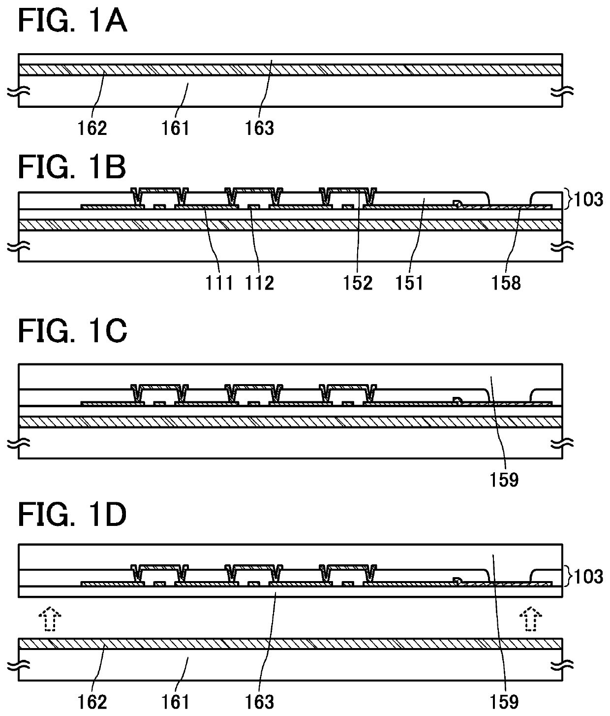
[0047]In this embodiment, a method for manufacturing a display device of one embodiment of the present invention is described with reference to drawings. In this embodiment, an example of a method for manufacturing a liquid crystal display device with a touch sensor is described.

[0048]First, a sensor layer 103 is formed over a support substrate 161 and separated from the support substrate 161. The steps up to here are described with reference to FIGS. 1A to 1D. Note that here, the case of using a projected capacitive touch sensor for the sensor layer 103 is described.

[0049]First, the support substrate 161 is prepared. As the support substrate 161, a substrate having a relatively flat surface is used. As the support substrate 161, a non-light-transmitting substrate such as a metal substrate or a ceramic substrate can be used in addition to a glass substrate or a resin substrate.

[0050]Next, a separation layer 162 and a layer to be separated 163 are stacked over the support substrate 1...

embodiment 2

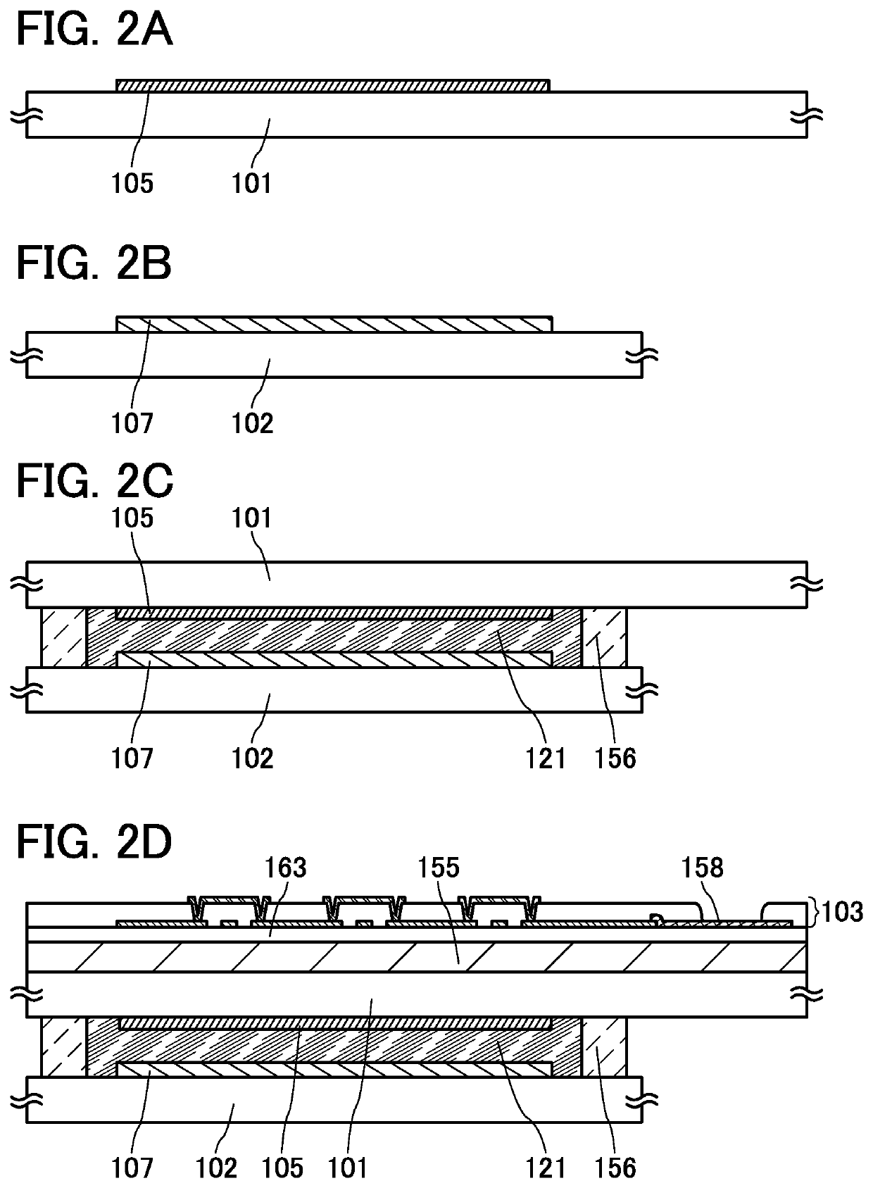
[0103]In this embodiment, a more specific structural example of a display device of one embodiment of the present invention is described with reference to drawings. Note that description of the same portions as those in the above embodiment is omitted in some cases.

example 1

Structural Example 1

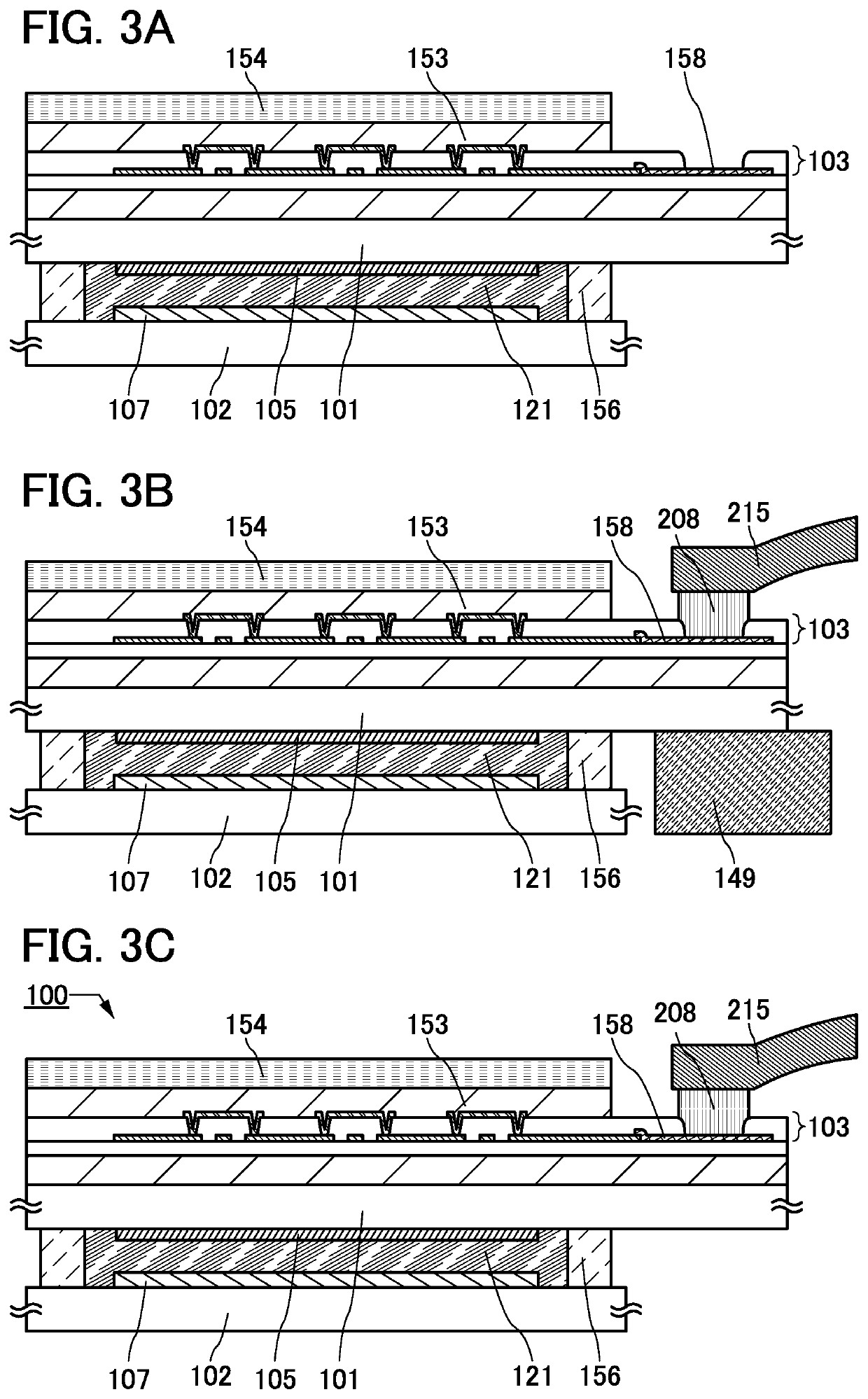
[0104]FIG. 5A is a schematic perspective view of a display device 200 described in this structural example. Note that FIGS. 5A and 5B illustrate only major components for simplicity. FIG. 5B is a developed perspective view schematically illustrating the display device 200.

[0105]The display device 200 includes a display portion 201 and a touch sensor 202. The display portion 201 is interposed between the first substrate 101 and the second substrate 102.

[0106]The second substrate 102 is provided with the display portion 201 and a plurality of wirings 206 electrically connected to the display portion 201. The plurality of wirings 206 is led to the periphery of the second substrate 102, and some of the wirings form part of an external connection electrode 205 for electrical connection to an FPC 204.

[0107]The display portion 201 includes a pixel portion 211 including a plurality of pixels, a source driver circuit 212, and a gate driver circuit 213. Although FIG. 5B il...


PUM

PropertyMeasurementUnit
angleaaaaaaaaaa
dew pointaaaaaaaaaa
thicknessaaaaaaaaaa

Abstract

To provide a thinned display device with a touch sensor and to provide a highly reliable display device. A sensor layer including an electrode of a touch sensor is formed in advance over a support substrate which is different from a substrate which forms a display device so that the sensor layer can be separated, the sensor layer is separated from the support substrate, and the separated sensor layer is attached to one surface of a substrate the other surface of which is provided with a component such as a color filter, with a bonding layer interposed therebetween.

Description

BACKGROUND OF THE INVENTION[0001]1. Field of the Invention[0002]The present invention relates to a display device with a touch sensor.[0003]2. Description of the Related Art[0004]A variety of electronic devices each including a display device, such as a cell phone, a smartphone, a personal computer, a tablet terminal, a portable game machine, and a portable music player, have recently come into widespread use. More intuitively operable electronic devices can be each obtained by providing a touch sensor so as to overlap with a display portion for image display as an interface of such an electronic device.[0005]In the display portion, a liquid crystal display device, a display device including an organic electroluminescent (EL) element, an electronic paper performing display by an electrophoretic method or the like, or the like can be typically used.[0006]Typical touch sensors are of resistive type and of capacitive type; besides, a variety of types such as a surface acoustic wave typ...

Claims


Application Information

Patent Timeline
Patent Type & Authority Patents(United States)
IPC IPC(8): G06F1/16G06F3/044G06F3/041G02F1/1333G06F3/14
CPCG06F3/1446G06F1/1643G06F1/1692G06F3/0412G06F3/0445G06F2203/04103G06F3/0446G06F3/044
Inventor HIRAKATA, YOSHIHARU
Owner SEMICON ENERGY LAB CO LTD
Why Eureka
Try Eureka