Frequency-selective metasurface integrated uncooled microbolometers

a metasurface and microbolometer technology, applied in the field of frequency-selective metasurface integrated uncooled microbolometers, can solve the problems of vox, spatial noise and complicated design, and relatively low frame rate of both materials, so as to improve equipment, minimize moving parts, and improve performance

Active Publication Date: 2021-09-14
UNIVERSITY OF MISSOURI
View PDF4 Cites 0 Cited by
  • Summary
  • Abstract
  • Description
  • Claims
  • Application Information

AI Technical Summary

Benefits of technology

[0007]The inventors have developed a better approach that integrates sensitivity into the microbolometer itself using a metasurface. At the same time, the performance is improved. Such integration of (e.g., wavelength) sensitivity into the microbolometer allows for incorporation into the ubiquitous uncooled microbolometer based FPA, and presents significant advantages via improved equipment, for example. Such advantages are analogous to the advantage that animals with color vision gain over those with intensity-only based vision (the ability to recognize predators / prey in hiding or identify ripe fruit). Another biological analogy is to the mantis shrimp that can resolve polarization. The wavelength sensitivity can be engineered to highlight battlefield hazards such as high explosives, chemical threats, or defeating enemy camouflage. For example, a single pixel in the FPA responds to radiation with a set of attributes (wavelength and polarization). This technique minimizes moving components in the assembly and preserves the uncooled / low-cost benefits of microbolometers.
[0008]Similar to wavelength sensitivity, polarization sensitivity helps to reveal the contrast between emitted radiation and reflected radiation. This is useful for identifying manmade tangents or signals. The ability to engineer sensitivity with coherence / angle-of-incidence (AOI) is critical for detecting illumination of a FPA with a laser source. This is useful if a laser is used to blind the FPA. It can also be used to build a plenoptic (light-field) camera which captures 3D information about a scene.
[0009]The present invention utilizes amorphous silicon germanium oxide (SixGeyO1-x-y). However, the interaction between the metasurface and sensing layer is also applicable to other materials, including α:Si and VOx). SixGeyO1-x-y has advantages because of its excellent IR radiation absorption, and mechanical and electrical properties at room temperature. The stoichiometry can be adjusted to maximize high temperature coefficient(s) of resistance (TCR) with a low resistivity and desired 1 / f noise. Thus, the device performance (responsivity and detectivity) is improved without increasing the 1 / f-noise. Because Si- and Ge-based compounds are standard materials in silicon integrated circuits, there is a wide range of established knowledge for fabrication of the microbolometer array. Such materials are also compatible with CMOS technology due to the low deposition temperature and the use of conventional dry-etch processing. Therefore, an FPA designed according to the novel approach herein can be easily integrated with readout electronics.
[0011]The inventors have investigated the structure / property relationships for metasurface integrated uncooled amorphous silicon germanium oxide (SixGeyO1-x-y) microbolometers, achieving disruptively lower voltage noise power spectral density (PSD) and higher voltage responsivity than conventional designs, while introducing the selectivity with respect to wavelength, polarization and AOI. Incorporating a metasurface into the microbolometer affects not only the conversion of electromagnetic (EM) energy to thermal energy, but also the thermal response and the electrical integration of the microbolometer. In addition, the presence of the metal metasurface elements significantly affects the tradeoff between resistivity and TCR, allowing the ability to obtain a film with high TCR with lower resistivity values than that of films without the metasurface. The inventors created a comprehensive model of the metasurfaces / microbolometer system as an integrated material with an engineered infrared, thermal and optical performance. By understanding the integrated material response, the inventors have facilitated better options for uncooled IR imaging. This includes optimization of the TCR, resistivity, and voltage noise of SixGeyO1-x-y thin films while enabling the metasurface performance. The inventors have also reduced microbolometer thickness (e.g., toward 50-60 nm Si—Ge—O) and pixel size to the lower thermal mass, and increased the FPA resolution.
[0012]The inventors have transformed current uncooled IR detectors by replacing the Fabry-Perot cavity / umbrella superstructure with a unified metasurface integrated microbolometer. The metasurfaces are used to determine spectral selectivity and be optimized to enhance electrical performance. This allows improved noise / sensitivity of the sensing material because it no longer needs to serve the dual function of absorbing the radiation. This allows the support structure to be designed to optimize the thermal isolation of the microbolometer and to facilitate measuring the resistance of the microbolometer without regard for disrupting the resonant cavity. Additionally, use of the lower resistivity of the metasurface integrated microbolometer improves TCR beyond the ordinary tradeoffs available for the Si—Ge—O system. This corresponds to lowering the noise of the microbolometers while maintaining or improving the sensitivity.
[0013]Moreover, the inventors have resolved the problematic issues of current detectors by fabricating supporting arms underneath the detector without disrupting the resonant cavity between the microbolometer pixel and a reflective mirror, and achieving a high fill factor. Noise-models were generated that can be applied to other IR detectors in order to resolve the common and difficult issues facing developers of IR detectors. Detection technology was developed in a simple, low cost, low power, light weight and portable system that operates at ambient temperature. For example, devices were fabricated with legs positioned underneath the microbolometer pixel without disrupting the ¼-wave resonance. This permits longer legs without sacrificing the fill factor in a focal plane array. The longer legs allow the thermal resistance between the microbolometer and the substrate. The metasurface also allows the IR absorption to be engineered with both broadband and narrowband designs. The inclusion of the metasurface improved the 1 / f noise by two orders of magnitude over an identical device with no metasurface. Additionally, the inventors developed metasurface integrated uncooled IR microbolometers for long wavelength detection. The inclusion of the metasurface permits engineering the IR absorptance with respect to wavelength, polarization, and AOI. Direct absorption by the metasurface removes the need for the ¼-wave cavity beneath microbolometer. In addition to benefiting the IR absorptance and architecture, the metasurface significantly improves the electrical performance of the temperature-sensing layer. Experimental results show an improvement in the TCR and a dramatic decrease in the resistivity. These parameters scale with the periodicity and area fraction of the metasurface.

Problems solved by technology

While VOx technology remains the standard, VOx presents issues when it is integrated into devices such as FPAs.
These challenges include spatial noise and complicated designs resulting from challenges integrating VOx into standard deposition equipment that is used in mainstream CMOS (complementary metal oxide semiconductor) and analog semiconductor fabrication.
Both materials have relatively low frame rates which limits the use of the systems to image fast moving objects and / or image from fast moving platforms.
In combination with slow frame rates, a limited number of pixels in FPAs also present a challenge for the use of microbolometers in IR hyperspectral detection applications, such as identification of gases and chemicals with low concentration, spectral filtering, defeating camouflage, and determining the absolute temperature of objects.
This is also due in part that most cameras use a standard ¼ wave cavity or other geometry to maximize the absorptance across the thermal infrared in ways that are not easy to make spectrally selective and to vary pixel-by-pixel.
For example, past experiments on tuning the cavity of a microbolometer, either through piezoelectric actuation, electrostatic actuation, liquid crystal based changes in the refractive index, or by using movable micromirror underneath the microbolometer pixel, have demonstrated the ability to tune the wavelength response at the expense of reduced FPA resolution and the complicated fabrication which dramatically increases the cost.
However, they are bulky and heavy due to the cryogenic cooling requirements, which thereby prevents their use in, for example, unmanned aerial vehicles (UAVs) or drones.

Method used


Image

  • Frequency-selective metasurface integrated uncooled microbolometers
  • Frequency-selective metasurface integrated uncooled microbolometers
  • Frequency-selective metasurface integrated uncooled microbolometers

Examples


Embodiment Construction

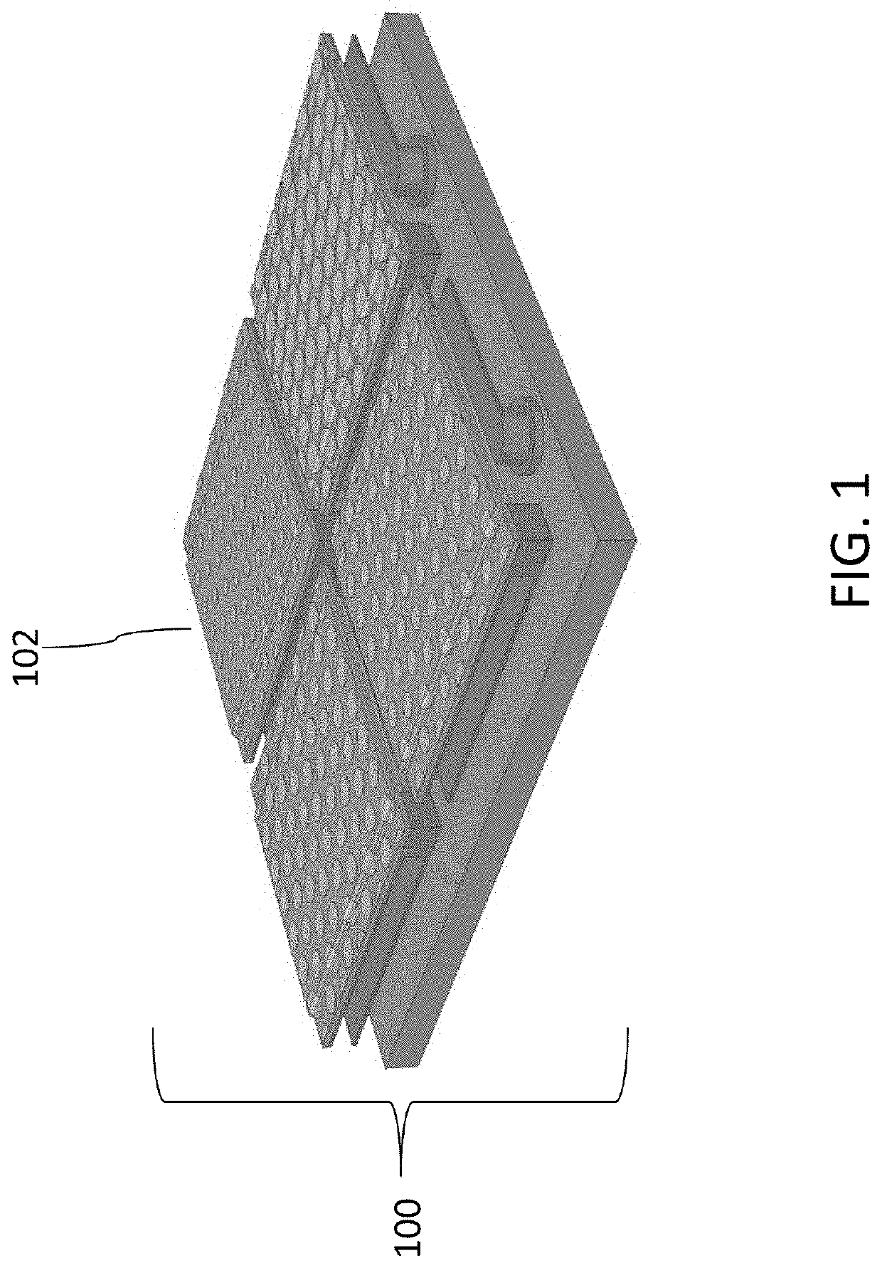
[0096]Metasurface integrated uncooled amorphous silicon germanium oxide (SixGeyO1-x-y) microbolometers include a metasurface, also known as an FSS, which is a periodic array of sub-wavelength antenna elements that establishes unusual properties from their structural design. FIG. 1 shows a microbolometer 100 including four pixels, of which pixel 102 represents one of the four pixels. The absorption at the IR frequencies is highly dependent on the metasurface geometry, and can be engineered for selectivity with respect to wavelength, polarization, and angle of incidence. EM energy with the correct characteristics is converted to heat, while other energy is reflected or transmitted away from the device. Metasurfaces can be coupled to a microbolometer platform, enabling an FPA to resolve these parameters. For example, one pixel can respond to horizontal polarized radiation while the adjacent pixels are sensitive to vertical or circular polarized radiation. Similarly, different microbolo...


PUM

PropertyMeasurementUnit
wavelengthsaaaaaaaaaa
thicknessaaaaaaaaaa
areaaaaaaaaaaa

Abstract

A metasurface integrated microbolometer having a sensing layer (e.g., SixGeyO1-x-y). The presence of the metasurface provides selectivity with respect to wavelength, polarization and angle-of-incidence. The presence of the metasurface into the microbolometer affects conversion of electromagnetic to thermal energy, thermal response, electrical integration of the microbolometer, and the tradeoff between resistivity and temperature coefficient of resistance, thereby allowing the ability to obtain a sensing with high temperature coefficient of resistance with lower resistivity values than that of films without the metasurface. The presence of the metasurface removes the need for a Fabry-Perot cavity.

Description

CROSS-REFERENCE TO RELATED APPLICATIONS[0001]This patent application claims priority to U.S. provisional patent application Ser. No. 62 / 659,001, filed Apr. 17, 2018, the entire disclosure of which is incorporated by reference herein.STATEMENT REGARDING FEDERALLY SPONSORED RESEARCH OR DEVELOPMENT[0002]This invention was made with government support under grants 1509589 and 1653792 awarded by the National Science Foundation and grant number W911NF-09-1-0158 awarded by the Army Research Office. The government has certain rights in the invention.BACKGROUND[0003]Uncooled microbolometers are used, for example, as infrared (IR) thermal sensors. In this application, the microbolometer absorbs IR radiation and is heated, raising its temperature. The temperature rise of the microbolometer is measured by measuring its electrical resistance. The temperature dependence of the resistivity is quantified by the Temperature Coefficient of Resistance (TCR). All other things being equal, a higher TCR ...

Claims


Application Information

Patent Timeline
Patent Type & Authority Patents(United States)
IPC IPC(8): G01J5/20G01J5/58H01L27/16H01L37/02
CPCG01J5/20G01J5/58H01L27/16H01L37/025G01J5/046G01J5/024G01J5/0853H10N19/00H10N15/15
Inventor ALMASRI, MAHMOUDKINZEL, EDWARD
Owner UNIVERSITY OF MISSOURI
Why Eureka
Try Eureka