
Semiconductor structure and method of forming the same

Active Publication Date: 2021-10-12
NAN YA TECH
View PDF7 Cites 0 Cited by
  • Summary
  • Abstract
  • Description
  • Claims
  • Application Information

AI Technical Summary

Benefits of technology

The patent text describes a way to improve the performance of a semiconductor structure by increasing its capacitance. This is achieved by etching the dielectric stack to expand the bottom portion of the opening, which prevents problems of under-etch and short-circuit. Overall, this method helps to create a higher-quality semiconductor structure.

Problems solved by technology

However, a problem of under-etch may occur when etching the dielectric stack to form the opening.
On the other hand, in order to avoid the problem of under-etch, the opening may be formed larger, and adversely causes the problem of short-circuit.

Method used


Image

  • Semiconductor structure and method of forming the same
  • Semiconductor structure and method of forming the same
  • Semiconductor structure and method of forming the same

Examples


Embodiment Construction

[0030]Reference will now be made in detail to the present embodiments of the disclosure, examples of which are illustrated in the accompanying drawings. Wherever possible, the same reference numbers are used in the drawings and the description to refer to the same or like parts.

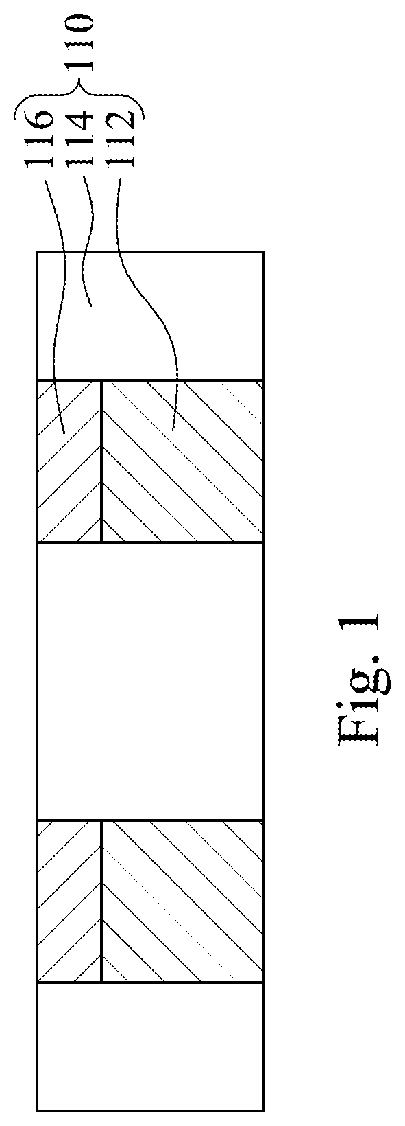
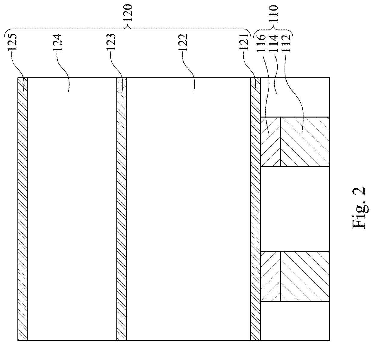
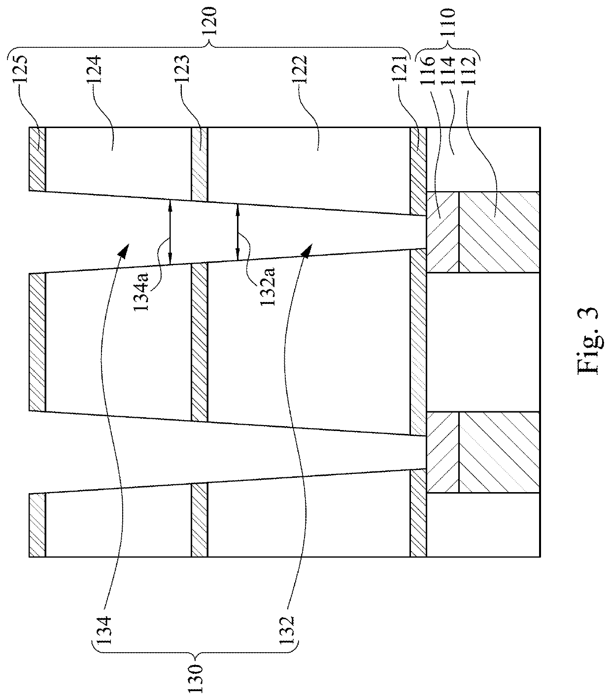
[0031]FIGS. 1 to 5 are cross-sectional views of a method of forming a semiconductor structure at various stages in accordance with some embodiments of the present disclosure.

[0032]Referring to FIG. 1, a substrate 110 is formed. The substrate 110 has an active region 112, an isolation structure 114 adjacent to the active region 112, and a contact 116 on the active region 112. In some embodiments, the active regions 112 may be made of silicon. The isolation structure 114 may be made of oxide, such as silicon oxide or other suitable material. The isolation structure 114 may be a shallow trench isolation (STI) structure. The contact 116 may be made of a conductive material, such as tungsten (W).

[0033]Referring to...


PUM


Abstract

A method of forming a semiconductor structure includes following steps. A substrate is formed. The substrate has an active region, an isolation structure adjacent to the active region, and a contact on the active region. A dielectric stack is formed on the substrate. The dielectric stack is etched to form an opening such that the contact of the substrate is exposed. The opening has a bottom portion and a top portion communicated to the bottom portion. The dielectric stack is etched again to expand the bottom portion of the opening.

Description

BACKGROUNDTechnical Field[0001]The present disclosure relates to a semiconductor structure and a method of forming the semiconductor structure.Description of Related Art[0002]Capacitors are used in a wide variety of semiconductor circuits. For example, the capacitors are used in DRAM (dynamic random access memory) memory circuits or any other type of memory circuit. DRAM memory circuits are manufactured by replicating millions of identical circuit elements, known as DRAM cells, on a single semiconductor wafer. A DRAM cell is an addressable location that can store one bit (binary digit) of data. In its most common form, a DRAM cell consists of two circuit components: a storage capacitor and an access field effect transistor.[0003]The development of the semiconductor circuits is to achieve larger capacitance, and thus an opening in a dielectric stack needs a smaller width. However, a problem of under-etch may occur when etching the dielectric stack to form the opening. On the other ha...

Claims


Application Information

Patent Timeline
IPC IPC(8): H01L27/108H01L49/02
CPCH01L27/1085H01L27/10805H01L28/60H01L28/82H10B12/03H10B12/30H01L28/90
Inventor WU, YEN-CHINGWANG, ROU-WEIJIA, SHUO
Owner NAN YA TECH
Learn More