TFT pixel threshold voltage compensation circuit with a source follower

a compensation circuit and source follower technology, applied in the field of electronic circuit design and operation, can solve the problems of non-uniform luminance, difficult to reduce further without degrading compensation accuracy, etc., and achieve the effect of eliminating hysteresis effects and reducing the hysteresis

Active Publication Date: 2021-11-09
SHARP KK
View PDF10 Cites 3 Cited by
  • Summary
  • Abstract
  • Description
  • Claims
  • Application Information

AI Technical Summary

Benefits of technology

[0014]There is a need in art, therefore, for an enhanced pixel circuit that provides for separate compensation and data programming phases to permit minimization of the one horizontal (1H) time, and accounts for variations in the voltage supply to enhance the uniformity of the display device output. Embodiments of the current application further improve over prior circuit configurations by (1) using a scan signal from another row to render unnecessary a dedicated data signal and associated additional control signal lines, which results in a narrower bezel; (2) removes the effects of data signal variations as a result of using the scan signal from another row; and (3) reduces the drive transistor hysteresis by applying a stress voltage at the gate and source of the drive transistor without employing additional complicated data line switches. The pixel circuits are capable of compensating the threshold voltage variations of the drive transistor with an ultra-short one horizontal time 1H of less than about 2 μs, which is shorter as compared to conventional configurations. In addition, the pixel circuit configurations described in the current application isolate the power supplies from the drive transistor. Any power supply variations, therefore, such as caused by an IR drop from the power supply to the drive transistor, will not affect the current to the OLED. An image having a generally uniform luminance thus can be displayed regardless of the voltage drop variations of the power supplies.
[0015]Embodiments of the present application provide pixel circuits for high refresh rate requirements, such as for 120 Hz applications. For such applications, an ultra-short 1H time (<2 μs) is achieved via separation of threshold compensation of the drive transistors and data programming phases. The threshold compensation time is dictated by the drive transistor characteristics and is difficult to reduce further without degrading the compensation accuracy. By separating the threshold compensation and data programming phases, a longer time can be allocated to threshold compensation for compensation accuracy. As referenced above, the RC constant time required for charging the programming capacitor is determinative of the programming time, and such programming time can be reduced to ultra-short 1H times (<2 μs).
[0017]In addition, an on bias stress transistor is incorporated that can electrically connect the first drive transistor to the power supply ELVDD during an on bias stress operation. During such operation, a voltage stress is applied to eliminate hysteresis effects associated with the drive transistor. The on bias stress operation may be performed as part of a refresh operation during which a data voltage is programmed to the pixel circuit, or as part of a low frequency operation during which a previously programming data voltage is maintained. The pixel circuit, therefore, is operable in two modes of operation including a refresh or normal operation, and low frequency or non-refresh operation. The normal or refresh operation is suitable for more dynamic images when the data voltage value is repeatedly being refreshed, whereas the low frequency or non-refresh operation is particularly suitable more static images when the data voltage value largely is remaining constant. Power consumption thus can be reduced.
[0018]In exemplary embodiments, low leakage transistors, such as IGZO (indium gallium zinc oxide) transistors, can be used as the switch transistors connected to respective voltage supply lines. By using low leakage transistors, either a low storage capacitor can be used to reduce the pixel size or a low refresh rate such as 30 Hz or lower can be used to better display static or low motion images.
[0019]An aspect of the invention, therefore, is a pixel circuit for a display device whereby the one horizontal time is minimized while maintaining accurate compensation of the threshold voltages of the drive transistors, and an on bias stress operation is performed to apply a voltage stress to eliminate hysteresis effects associated with the drive transistor. In exemplary embodiments, the pixel circuit includes a first drive transistor configured to control an amount of current to a light-emitting device during an emission phase depending upon a voltage applied to a gate of the first drive transistor, the first drive transistor having a first terminal and a second terminal; a second drive transistor that is configured as a source follower relative to the first drive transistor, wherein a first terminal of the second drive transistor is connected to a first power supply line and a second terminal of the second drive transistor is connected to the second terminal of the first drive transistor; wherein the first drive transistor is one of a p-type or n-type transistor and the second drive transistor is the other of a p-type or n-type transistor; a light-emitting device that is electrically connected at a first terminal to the first terminal of the first drive transistor during the emission phase and is connected at a second terminal to a second power supply line; and an on bias stress switch transistor having a first terminal connected to the first power supply line and the first terminal of the second drive transistor, and a second terminal connected to a node Vx that is a connection of the second terminal of the first drive transistor and the second terminal of the second drive transistor, wherein when the on bias stress switch transistor is in an on state the first power supply line is electrically connected to the node Vx to apply a voltage stress to eliminate hysteresis effects.
[0021]The pixel circuit is operable to perform a refresh operation in which the pixel circuit is programmed with a data voltage for the emission phase, wherein during the data programming phase an on bias stress operation is performed to eliminate hysteresis effects. The pixel circuit also is operable to perform a low frequency operation during which a previously programmed data voltage is maintained, wherein the low frequency operation includes resetting an anode of the light-emitting device and performing an on bias stress operation to eliminate hysteresis effects, and then returning to the emission phase. The low frequency operation may be performed multiple times periodically following one refresh operation to generate a more static image.

Problems solved by technology

The threshold compensation time is dictated by the drive transistor characteristics and is difficult to reduce further without degrading the compensation accuracy.
Hence, any IR drop on the power supply ELVDD line will not cause non-uniform luminance.

Method used


Image

  • TFT pixel threshold voltage compensation circuit with a source follower
  • TFT pixel threshold voltage compensation circuit with a source follower
  • TFT pixel threshold voltage compensation circuit with a source follower

Examples


Embodiment Construction

[0029]Embodiments of the present application will now be described with reference to the drawings, wherein like reference numerals are used to refer to like elements throughout. It will be understood that the figures are not necessarily to scale.

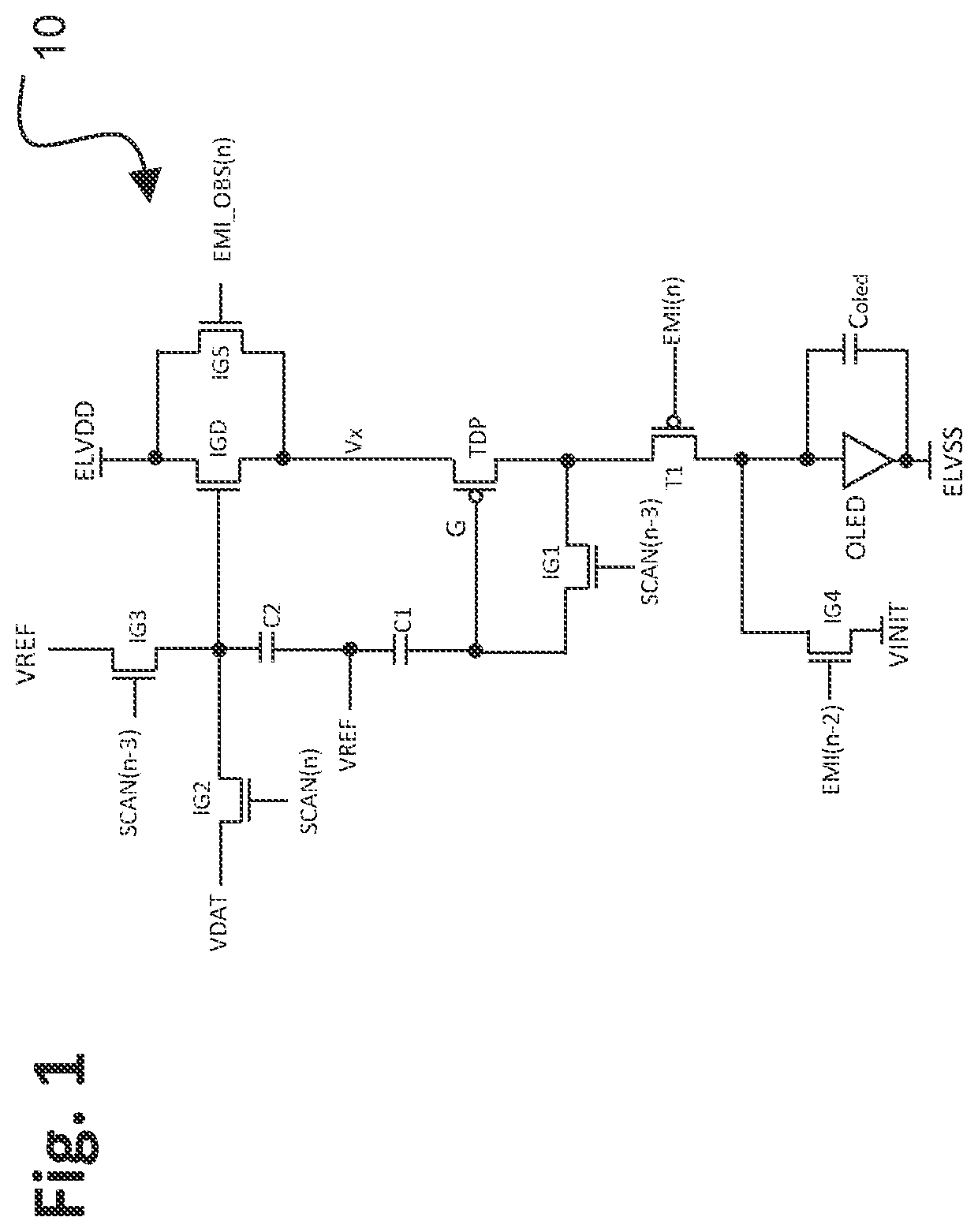
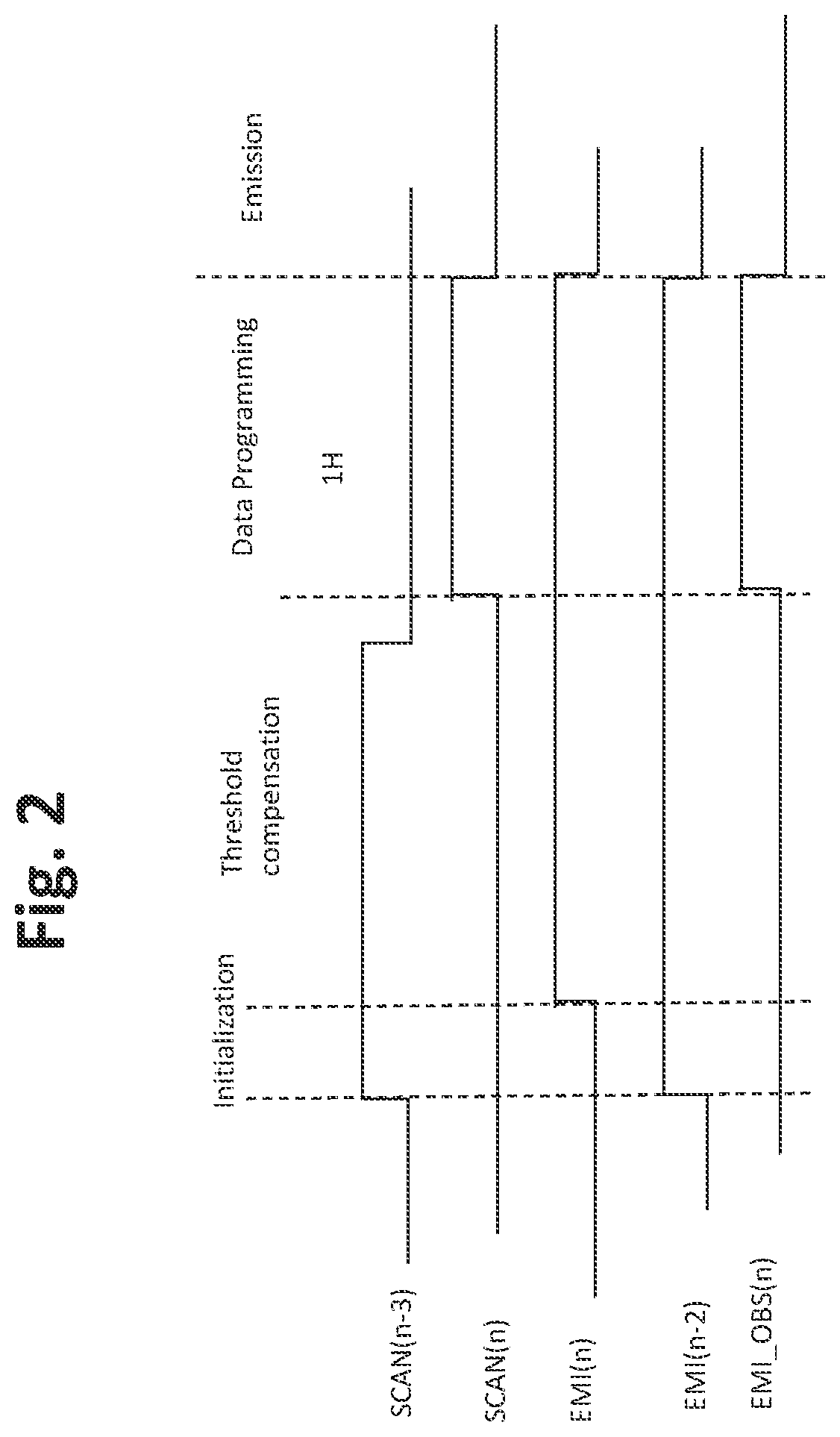
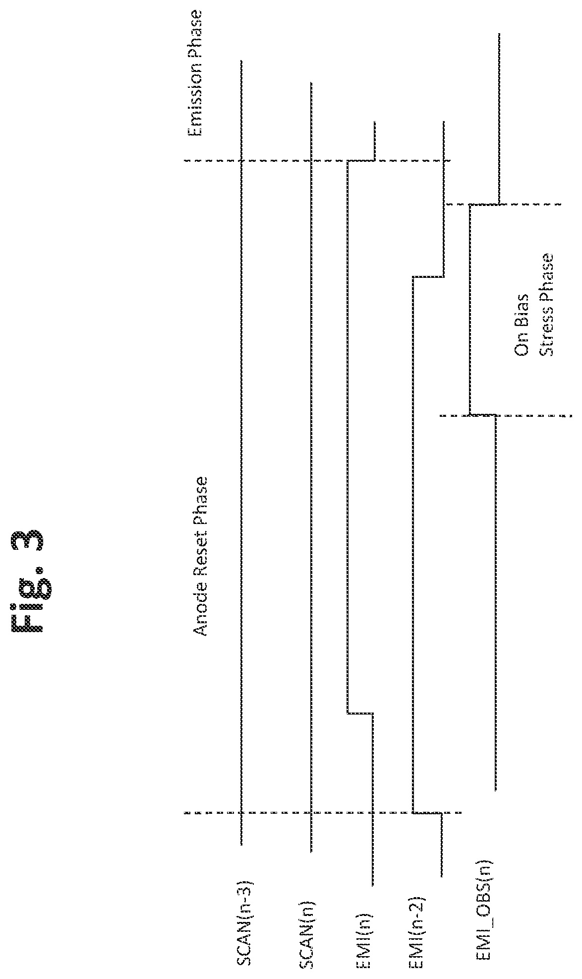
[0030]FIG. 1 is a drawing depicting a first circuit configuration 10 in accordance with embodiments of the present application, and FIG. 2 is a timing diagram associated with the operation of the circuit configuration 10 of FIG. 1 that is associated with a normal or refresh operation. FIG. 3 is a drawing depicting a timing diagram associated with the operation of the circuit of FIG. 1 that is suitable for low frequency or non-refresh operation.

[0031]In this example, the circuit 10 is configured as a thin film transistor (TFT) circuit that includes multiple p-type transistors TDP and T1, multiple n-type transistors IGD and IG1˜IG5, and two storage capacitors C1 and C2. In exemplary embodiments, the p-type transistors are low-temperature polyc...


PUM


Abstract

An enhanced pixel circuit for a display device provides separate compensation and data programming phases to permit minimization of the programming time. Variations in voltage supplies are accounted for by isolating the drive transistor from such power supply by using a second drive transistor configured as source follower relative to the first drive transistor. An on bias stress transistor is incorporated that can electrically connect the first drive transistor to the power supply during an on bias stress operation. During such operation, a voltage stress is applied to eliminate hysteresis effects associated with the drive transistor. The on bias stress operation may be performed as part of a refresh operation during which a data voltage is programmed to the pixel circuit, or as part of a low frequency operation during which a previously programming data voltage is maintained which reduces power consumption.

Description

TECHNICAL FIELD[0001]The present application relates to design and operation of electronic circuits for delivering electrical current to an element in a display device, such as for example to an organic light-emitting diode (OLED) in the pixel of an active matrix OLED (AMOLED) display device.BACKGROUND ART[0002]Organic light-emitting diodes (OLED) generate light by re-combination of electrons and holes, and emit light when a bias is applied between the anode and cathode such that an electrical current passes between them. The brightness of the light is related to the amount of the current. If there is no current, there will be no light emission, so OLED technology is a type of technology capable of absolute blacks and achieving almost “infinite” contrast ratio between pixels when used in display applications.[0003]Several approaches are taught in the prior art for pixel thin film transistor (TFT) circuits to deliver current to an element of a display device, such as for example an o...

Claims


Application Information

Patent Timeline
Patent Type & Authority Patents(United States)
IPC IPC(8): G09G3/30G09G3/3258G09G3/3291H01L27/32G09G3/20
CPCG09G3/3258G09G3/2092G09G3/3291H01L27/3262H01L27/3265G09G2330/021G09G3/3225G09G3/3233G09G2300/0819G09G2300/0861G09G2320/045G09G2310/0262G09G2300/0852G09G2340/0435G09G2320/103G09G2310/08H10K59/12H10K59/1213H10K59/1216
Inventor LU, TONGTANAKA, KOHHEI
Owner SHARP KK
Why Eureka
Try Eureka