Nanopore FET sensor with non-linear potential profile

a non-linear potential and sensor technology, applied in the field of nanopore field-effect transistor (fet) sensors, can solve the problems of preventing the move towards higher throughput and robustness, none can solve all challenges, and lack of silicon platform maturity

Active Publication Date: 2022-06-21
INTERUNIVERSITAIR MICRO ELECTRONICS CENT (IMEC VZW)
View PDF6 Cites 0 Cited by
  • Summary
  • Abstract
  • Description
  • Claims
  • Application Information

AI Technical Summary

Benefits of technology

[0011]It is an advantage of embodiments of the present invention that a nanopore field-effect transistor sensor with a large sensitivity (e.g. sufficient to identify single molecules) can be obtained.
[0012]It is an advantage of embodiments of the present invention that a nanopore field-effect transistor sensor with a high spatial resolution (e.g. sufficient to identify single nucleotides in a DNA strand) can be obtained.
[0013]It is an advantage of embodiments of the present invention that a relatively large number (e.g. an array) of nanopore field-effect transistor sensors can be formed on a single substrate. It is yet a further advantage of embodiments of the present invention that a relatively large number of sensing actions, of the same or of different analyte solutions, can be performed simultaneously; thereby speeding up the overall measurement to increase the throughput or achieving a higher accuracy in the same time span. It is a further advantage of embodiments of the present invention that the malfunction of a nanopore field-effect transistor in the plurality of nanopore field-effect transistor working in parallel can have a low effect on the overall performance of the device.
[0014]It is an advantage of embodiments of the present invention that the nanopore field-effect transistor sensor may be relatively inexpensive to manufacture, even in large numbers.
[0015]It is an advantage of embodiments of the present invention that the nanopore field-effect transistor sensor can be made using well-known techniques from semiconductor technology (e.g. CMOS technology). It is a further advantage of embodiments of the present invention that the nanopore field-effect transistor sensor can be made in a way that is compatible with other semiconductor devices and that they can be integrated therewith on a single substrate.

Problems solved by technology

Revealing this sequence, however, requires the solving of several fundamental problems.
However, drawbacks of this technique are the susceptible lipid membrane and bio-nanopores and the weak current signals (˜pA) preventing the move towards higher throughput and robustness.
Different solid-state nanopore technologies have been developed and show feasibility on single-molecular sensing, but none can solve all challenges, especially the intrinsic conflicts between current intensity, spatial resolution, and sensitivity.
Although these materials indeed have very interesting properties, they still lack the maturity of the silicon platform, making it difficult to achieve a parallelized read-out scheme with millions of nanopores per chip.

Method used


Image

  • Nanopore FET sensor with non-linear potential profile
  • Nanopore FET sensor with non-linear potential profile
  • Nanopore FET sensor with non-linear potential profile

Examples


example 1

Fabrication of an Asymmetric Nanopore Field-Effect Transistor Sensor

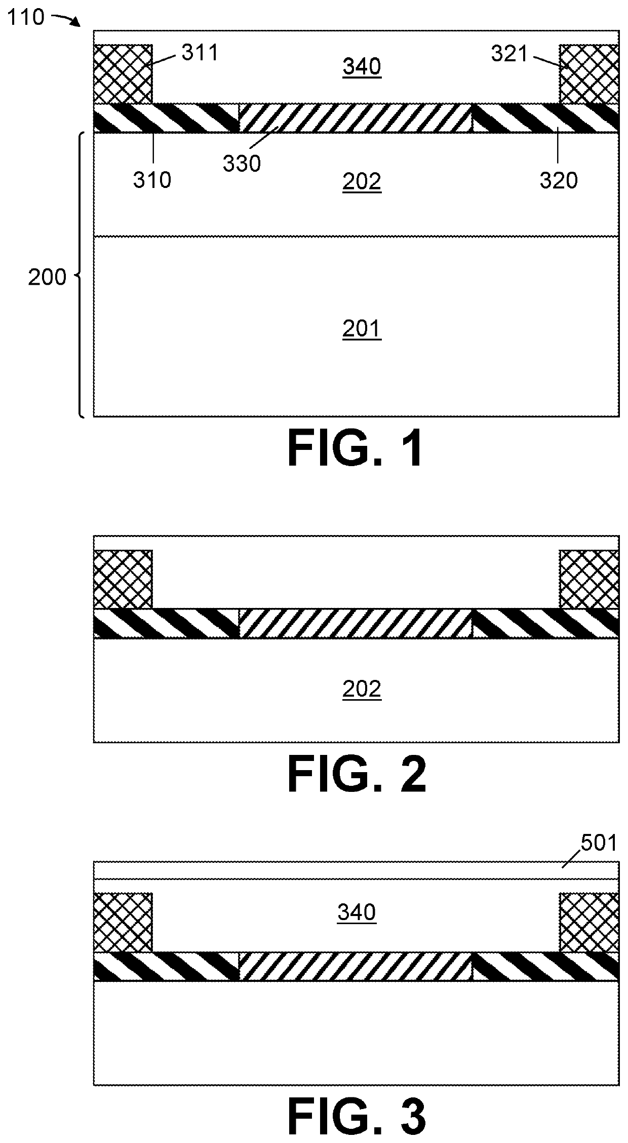
[0162]We now refer to FIG. 1. A field-effect transistor (FET) structure (110) is first provided comprising a substrate (200) comprising a buried oxide layer (202; e.g. SiO2) on a support layer (201), a channel region (330) on the buried oxide layer (202) in-between two source / drain regions (310,320), source / drain contacts (311,321) to the source / drain regions (310,320) and a dielectric layer (340) conformally covering the channel region (330), source / drain regions (310,320) and source / drain contacts (311,321). This FET structure (110) may be made based on methods which are well-known in the art.

[0163]We now refer to FIG. 2. A deep (e.g. around 50 to 100 μm deep) dry or wet etching is performed to open the bottom of the buried oxide layer (202), through the support layer (202). A freestanding FET structure is thereby obtained.

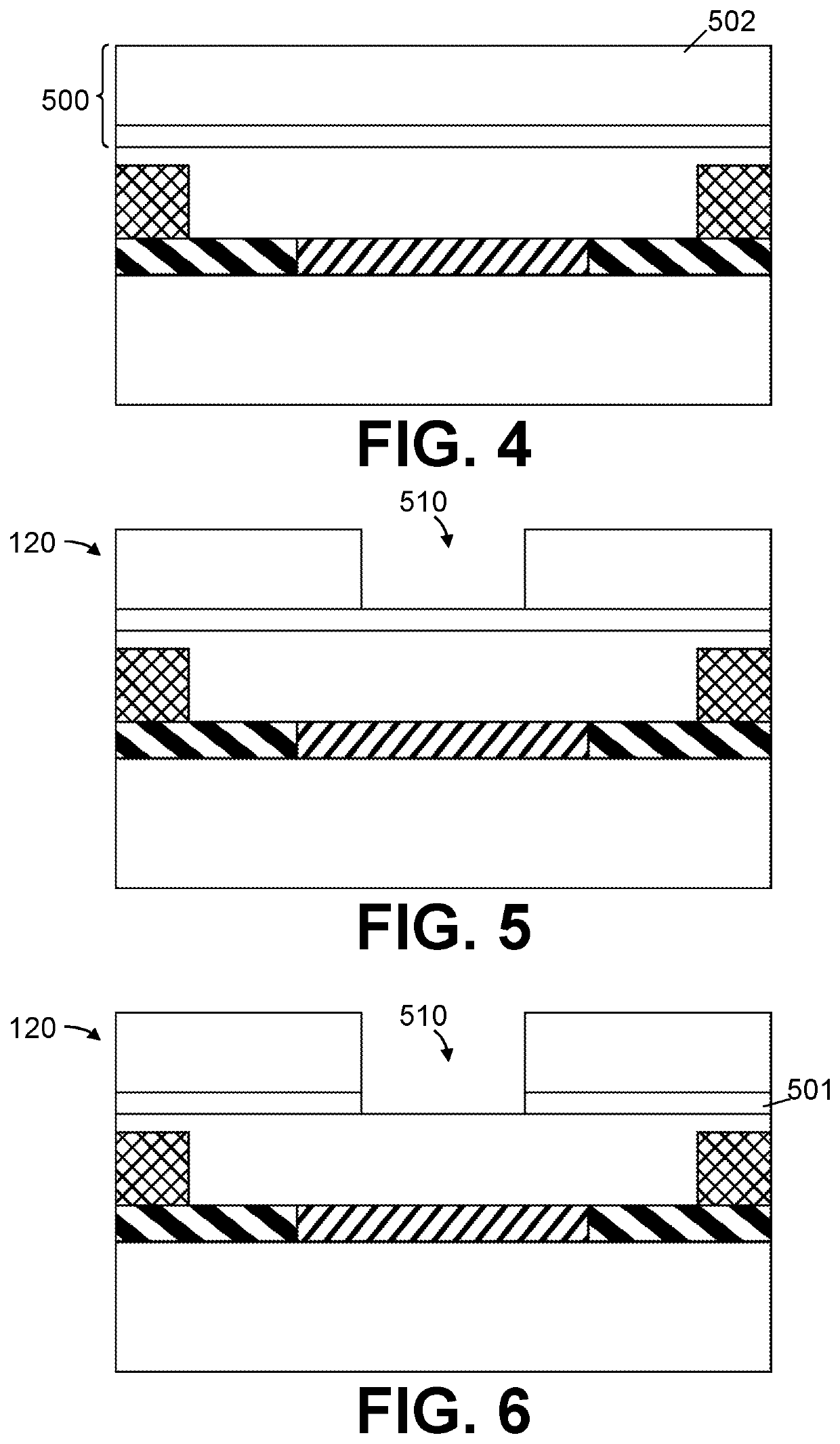
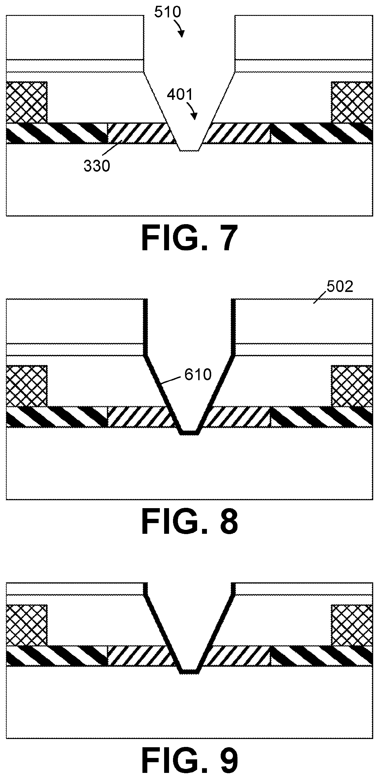
[0164]We now refer to FIG. 3. A hardmask layer (501) (e.g. Al2O3) is deposited over the diel...

example 2

Various Asymmetric Nanopore Architectures Suitable for Creating a Non-Linear Potential Profile

[0179]The architecture of a nanopore can typically be decomposed into at least the vertical profile of the nanopore and the shape of its orifices.

[0180]We now refer to FIG. 15, parts a-d, showing vertical cross-sections of various exemplary asymmetric nanopore (400) profiles in accordance with embodiments of the present invention. In FIG. 15, part a, a nanopore (400) having a width which tapers uniformly from the first orifice (410) to the second orifice (420) is shown. In FIG. 15, part b, a nanopore (400) with a step-profile is shown; e.g. the width (w) of the nanopore (400) may have one or more discrete locations at which the nanopore width changes, but said width may otherwise be relatively constant. In FIG. 15, part c, a nanopore (400) is shown having a constant width, but comprising subcomponents (431,432) of differing composition; the subcomponents (431,432) may, for example, have a d...

example 3

Effect of a Non-Linear Potential Profile

[0189]We now refer to FIG. 17, depicting characteristic potential profile curves for 20 nm long nanopores, going from their entrance (i.e. the cis orifice; Z=0 nm) to their exit (i.e. the trans orifice; Z=20 nm). The potential profile (701, 702, 703) of a symmetric nanopore (701) having a uniform width and nature across the entire depth, a step-profile asymmetric nanopore (702) and a uniformly tapering asymmetric nanopore (703) are shown, both in an empty (i.e. containing a fluid, but no analyte; full line) and filled (i.e. containing an analyte; dashed line) state. As shown in FIG. 17, the potential profile of the symmetric nanopore barely differs between the filled state and the empty state (very small ΔAV1), complicating the detection of the presence of the analyte. Conversely, for both asymmetric nanopores, the potential profile in the filled state is considerably different from that in the empty state (large ΔV2 and ΔV3); e.g. a differenc...


PUM

PropertyMeasurementUnit
ionic currentaaaaaaaaaa
lengthaaaaaaaaaa

Abstract

In a first aspect, the present invention relates to a nanopore field-effect transistor sensor (100), comprising: i) a source region (310) and a drain region (320), defining a source-drain axis; ii) a channel region (330) between the source region (310) and the drain region (320); iii) a nanopore (400), defined as an opening in the channel region (330) which completely crosses through the channel region (330), oriented at an angle to the source-drain axis, having a first orifice (410) and a second orifice (420), and being adapted for creating a non-linear potential profile between the first (410) and second (420) orifice.

Description

CROSS-REFERENCE[0001]This application is a 371 U.S. national phase of PCT / EP2018 / 070007, filed Jul. 24, 2018, which claims priority from EP 17210422.6, filed Dec. 22, 2017, both which are incorporated by reference in its entirety.TECHNICAL FIELD OF THE INVENTION[0002]The present invention relates to the field of field-effect transistor (FET) sensors; more particularly to nanopore field-effect transistor sensors.BACKGROUND OF THE INVENTION[0003]Biosensors have been developed intensively during the last decades and have enabled a wide set of applications in life sciences. As a very special biosensors, nanopore sensors provide the unique advantage of single molecule sensitivity; thereby having a great potential for single molecule studies and DNA sequencing. A first sequencing strategy by means of a nanopore is based on electrophoresis driven DNA translocation through the nanopore and subsequently monitoring the blockade effect of DNA on the ionic current flow through this nanopore. Th...

Claims


Application Information

Patent Timeline
Patent Type & Authority Patents(United States)
IPC IPC(8): H01L21/00H01L29/786G01N27/414H01L21/308H01L29/10H01L29/51
CPCH01L29/78696G01N27/4146H01L21/308H01L29/1041H01L29/511G01N33/48721
Inventor CHEN, CHANGMARTENS, KOENVAN DORPE, POLSEVERI, SIMONE
Owner INTERUNIVERSITAIR MICRO ELECTRONICS CENT (IMEC VZW)
Why Eureka
Try Eureka