
LCD device and OLED display device

a display device and liquid crystal display technology, applied in the field of displays, can solve the problems of severe signal noise, adversely affecting the acquisition of fingerprint recognition sensor signals, and no liquid crystal display (lcd)-based under-screen fingerprint recognition products

Active Publication Date: 2022-09-20
WUHAN CHINA STAR OPTOELECTRONICS TECH CO LTD
View PDF8 Cites 0 Cited by
  • Summary
  • Abstract
  • Description
  • Claims
  • Application Information

AI Technical Summary

Benefits of technology

The present invention provides an LCD device with a liquid crystal lens and fingerprint recognition sensor for improved fingerprint touch. The liquid crystal lens has holes to improve reflected light from fingerprints and optimize imaging quality. In OLED display devices, a two-layered liquid crystal lens structure is used to reduce the sensor's signal receiving area and manufacturing costs. The liquid crystal lens structure is driven in a time-sharing manner to reduce power consumption and impact on display during normal display, except for fingerprint recognition, when it becomes the lens. This technology advancement improves the accuracy and comfort of fingerprint touch on LCD and OLED display devices.

Problems solved by technology

However, there is currently no liquid crystal display (LCD)-based under-screen fingerprint recognition products.
But light reflection also occurs when pixel opening areas are covered by a fingerprint, and light intensity of light passing through the opening areas is much greater than light intensity of light passing through the holes, thereby causing severe signal noise and adversely affecting acquisition of fingerprint recognition sensor signals.
Under-screen fingerprint recognition can even be failed when accuracy of the sensors is not good enough.
In addition, micro lenses have large volume, heavy weight, single shape, and are fragile.
Besides, for micro lenses, module design is difficult, mass production is hard to be achieved, production efficiency is low, and manufacturing costs are high.
Because under normal circumstances, a refractive index of an adhesive (such as optical clear adhesive, OCA) is relatively close to a refractive index of the lens, thereby significantly reducing performance of the lenses or even rendering the lenses ineffective.

Method used


Image

  • LCD device and OLED display device
  • LCD device and OLED display device
  • LCD device and OLED display device

Examples


embodiment 1

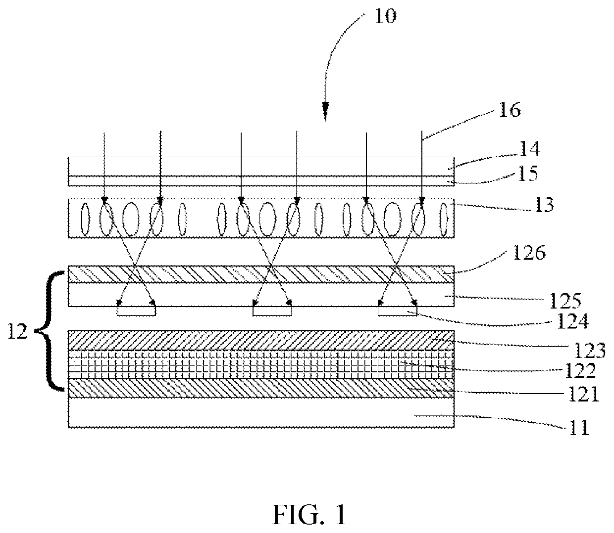
[0038]Please refer to FIG. 1 showing a schematic structural view of an LCD device 10 in accordance with the first embodiment of the present invention. The LCD device 10 is provided with a backlight module 11 disposed at a bottom of the LCD device 10. A bottom polarizer 121 is disposed on the backlight module 11. A TFT layer and a TFT trace 122 are fabricated on the bottom polarizer 121. Then, a liquid crystal layer 123 is fabricated on the TFT layer and the TFT trace 122. A color filter plate 125 is disposed on the liquid crystal layer 123. A fingerprint recognition sensor 124 is provided below the color filter plate 125. A top polarizer 126 is disposed on the color filter plate 125.

[0039]The bottom polarizer 121, the TFT layer and the TFT trace 122, the liquid crystal layer 123, the color filter plate 125, the fingerprint recognition sensor 124, and the top polarizer 126 cooperatively constitute a display module 12. A liquid crystal lens layer 13 is disposed above the display modul...

embodiment 2

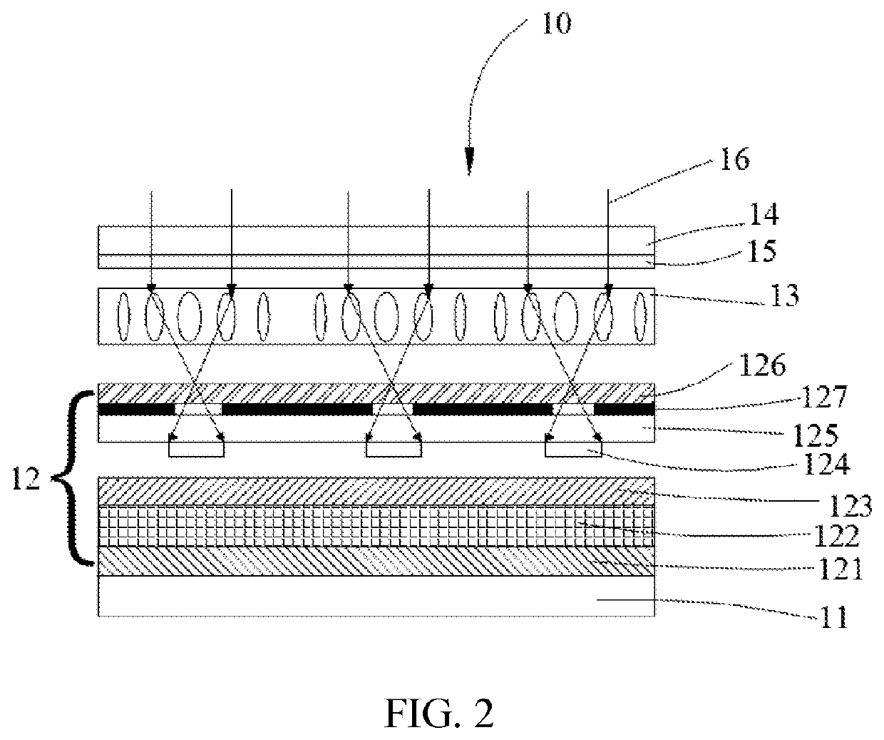
[0043]Please refer to FIG. 2 showing a schematic structural view of an LCD device 10 in accordance with the second embodiment of the present invention. In comparison with the LCD display device 10 in the first embodiment, the LCD display device 10 in the second embodiment is provided with a black mask layer 127 disposed on the color filter plate 125 in the display module 12.

[0044]The lens array of the liquid crystal lens layer 13 corresponds to an array of holes formed by the black mask layer 127. By using lens focusing and pinhole imaging, a utilization of reflected light reflected by a finger can be maximized, thereby increasing recognizability of fingerprint touch. The black mask layer 127 is a black matrix or is made of a black metal, such as metal aluminum and molybdenum oxide.

[0045]The black mask layer 127 is disposed on the color filter plate 125, and is preferably disposed on an upper surface of the color filter plate 125. A position of stacking the black mask layer 127 in a...

embodiment 3

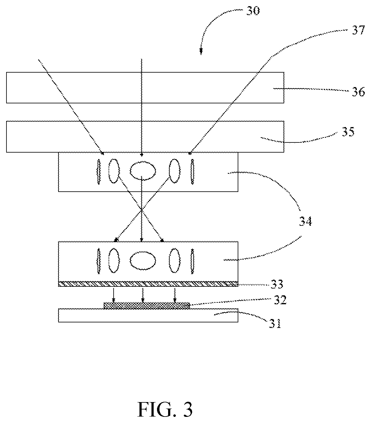
[0046]Please refer to FIG. 3 showing a schematic structural view of an organic light-emitting diode (OLED) display device 30 in accordance with a third embodiment of the present invention. The third embodiment is directed to an OLED display device 30. The OLED display device 30 includes a base substrate and a base substrate trace 31 disposed on a bottom of the OLED display device 30. A fingerprint recognition unit 32 is disposed on the base substrate and the base substrate trace 31. A two-layered liquid crystal lens layer 34 is disposed above the fingerprint recognition unit 32. An OLED display 35 is disposed on the two-layered liquid crystal lens layer 34. A cover glass 36 is disposed on the OLED display.

[0047]The fingerprint recognition unit of the OLED display device includes a fingerprint recognition sensor.

[0048]The two-layered liquid crystal lens layer 34 is configured to operate in a lens state when the fingerprint recognition unit is operating, and two-layered liquid crystal...


PUM

PropertyMeasurementUnit
wavelengthaaaaaaaaaa
light transmittanceaaaaaaaaaa

Abstract

A liquid crystal display (LCD) device and an organic light-emitting diode (OLED) display device are disclosed. The LCD device includes a base substrate, a display module, and a liquid crystal lens layer. The display module includes a fingerprint recognition sensor. The OLED display device includes a base substrate, a fingerprint recognition sensor, a two-layered liquid crystal lens layer, and an OLED display. The liquid crystal lens layer is configured to be switchable between a non-lens state and a lens state. By adopting liquid crystal lenses with holes, utilization of reflected light reflected by a fingerprint can be improved and imaging quality can be optimized.

Description

BACKGROUND OF INVENTION1. Field of Invention[0001]The present invention relates to a technical field of displays, and particularly to, a liquid crystal display device and an organic light-emitting diode device.2. Related Art[0002]With ever-changing technologies, a trend in development is turning to full-screen mobile terminals. Fingerprint recognition technologies are widely used in mobile phones, tablets, televisions, access control, and safes due to their development. Fingerprint recognition technologies mainly include optical, capacitive, and ultrasonic types. Among them, optical fingerprint recognition technology provides a wider range of recognition and lower cost. Under-screen fingerprint recognition technology in full-screen mobile terminals has become a standard specification for flagship models of major brands of mobile phones. However, there is currently no liquid crystal display (LCD)-based under-screen fingerprint recognition products.[0003]Based on LCD under-screen fing...

Claims


Application Information

Patent Timeline
Patent Type & Authority Patents(United States)
IPC IPC(8): G02F1/137G06V40/13G02F1/1333G02F1/1335G02F1/1343G02F1/1368H01L27/32G06V10/145G06F3/0354G06K9/00
CPCG02F1/13793G02F1/1368G02F1/13338G02F1/133512G02F1/133514G02F1/133526G02F1/133528G02F1/134309G06V40/1318H01L27/3232G06F3/03547G06K9/00G06V10/145G02F1/1333G02F1/1347G02F1/137G02F1/133308G02F1/1343G02F1/13332G06V40/12H10K59/65G02F1/294H10K59/50
Inventor ZHA, GUOWEILIU, FANCHENG
Owner WUHAN CHINA STAR OPTOELECTRONICS TECH CO LTD
Learn More