Laser irradiation apparatus and method of fabricating a semiconductor device

a laser irradiation and semiconductor technology, applied in the direction of semiconductor lasers, active medium materials, instruments, etc., can solve problems such as interfering with each other

Inactive Publication Date: 2001-06-28
SEMICON ENERGY LAB CO LTD
View PDF0 Cites 116 Cited by
  • Summary
  • Abstract
  • Description
  • Claims
  • Application Information

AI Technical Summary

Problems solved by technology

The cause of the interference patterns seen in the film resides in that the laser beam is split an

Method used


Image

  • Laser irradiation apparatus and method of fabricating a semiconductor device
  • Laser irradiation apparatus and method of fabricating a semiconductor device
  • Laser irradiation apparatus and method of fabricating a semiconductor device

Examples


embodiment 1

(Embodiment 1)

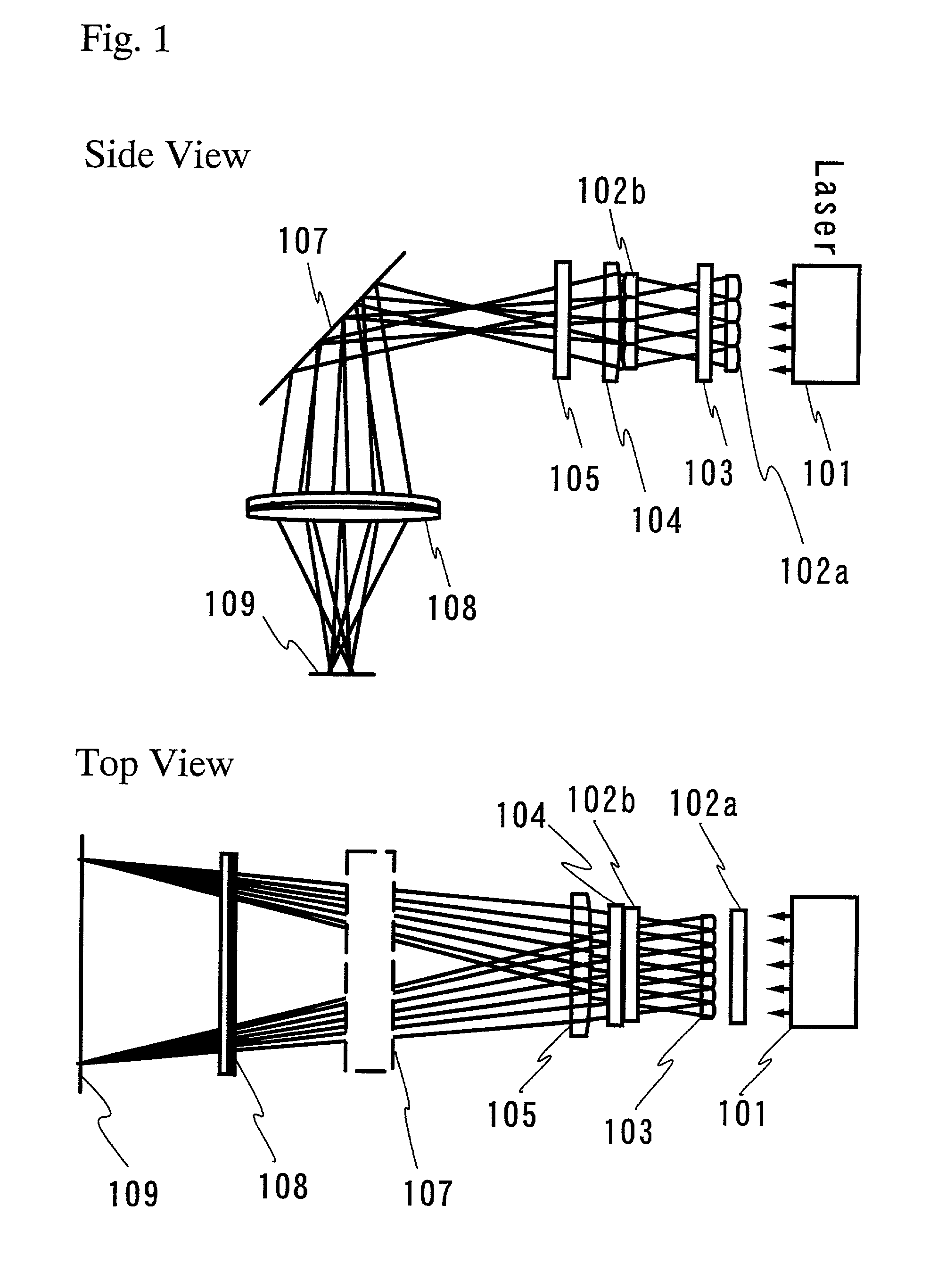
[0089] In this embodiment, a case where irradiation is made using an excimer laser will be described. The basic structure of a laser irradiation apparatus of this embodiment is the same as FIG. 3, and the positions of respective mirrors in a mirror of the invention are concretely calculated and are shown in FIG. 11. In FIG. 11, a plane perpendicular to an irradiation surface and parallel to the width direction of a beam is made an xy plane, and the longitudinal direction of the beam is made a z axis. Here, for simplifying the explanation of a mirror 1101, it is assumed that the mirror 1101 and an irradiation surface 1105 are disposed at z=0.

[0090] The mirror 1101 is made of a plurality of plane mirrors 1102 to 1104. The plane perpendicular to the irradiation surface and parallel to the width direction of the beam is made the xy plane, and the longitudinal direction of the beam is made the z axis. Here, for simplifying the explanation of the mirror 1101, it is assumed t...

embodiment 2

(Embodiment 2)

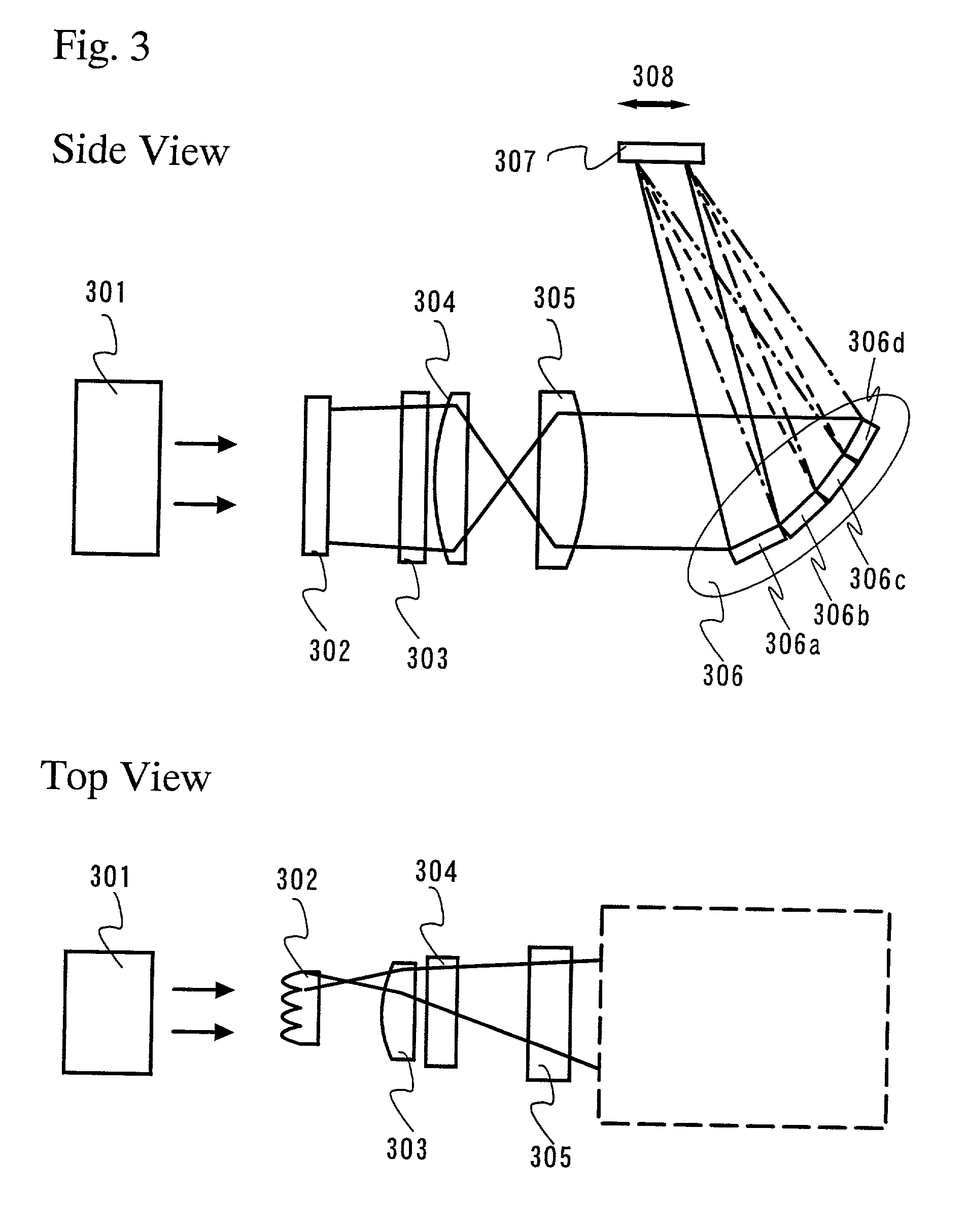
[0104] In this embodiment, a description will be made on a case where irradiation is made using a YAG laser. Although the basic structure of a laser irradiation apparatus of this embodiment is the same as FIG. 9, positions of mirrors are concretely calculated.

[0105] Since the coherent length of the YAG laser is longer than the coherent length of the excimer laser, the interference can not be suppressed very much by only shifting a mirror by 1 mm as in FIG. 12 of Embodiment 1. Thus, it is better to shift a mirror by about 10 mm as in FIG. 13.

[0106] Similarly to Embodiment 1, coordinates of both ends in the width direction of a laser beam on an irradiation surface 1306 are made (0, 200) and (0, 199). Since it is desired that an actual laser beam width is made about 1 mm, the coordinate is also made such. An arbitrary point is made (x.sub.0, y.sub.0)=(200, 190), and similarly to Embodiment 1, when an attempt is made to obtain (x.sub.1, y.sub.1) by using the expressions (1...

embodiment 3

(Embodiment 3)

[0108] This embodiment will be described with reference to FIGS. 15A to 21. Here, a method of fabricating a pixel TFT of a display region and a TFT of a driver circuit provided at the periphery of the display region on the same substrate, and a display device using the same, will be described in detail in accordance with a fabricating process. However, for simplification of the explanation, a CMOS circuit as a basic circuit of a shift register circuit, a buffer circuit, or the like in a control circuit and an n-channel TFT forming a sampling circuit will be shown in the drawings.

[0109] In FIG. 15A, as a substrate 1501, a low alkaline glass substrate or a quartz substrate can be used. In this embodiment, the low alkaline glass substrate was used. An under film 1502, such as a silicon oxide film, a silicon nitride film, or a silicon nitride oxide film, for preventing impurity diffusion from the substrate 1501 is formed on the surface of this substrate 1501 on which the T...


PUM

PropertyMeasurementUnit
Lengthaaaaaaaaaa
Shapeaaaaaaaaaa

Abstract

There is provided an optical system for reducing faint interference observed when laser annealing is performed to a semiconductor film. The faint interference conventionally observed can be reduced by irradiating the semiconductor film with a laser beam by the use of an optical system using a mirror of the present invention. The optical system for transforming the shape of the laser beam on an irradiation surface into a linear or rectangular shape is used. The optical system may include an optical system serving to convert the laser beam into a parallel light with respect to a traveling direction of the laser beam. When the laser beam having passed through the optical system is irradiated to the semiconductor film through the mirror of the present invention, the conventionally observed faint interference can be reduced. Besides, the optical system which has been difficult to adjust can be simplified.

Description

[0001] 1. Field of the Invention[0002] The present invention relates to an apparatus for manufacturing a semiconductor device having a circuit structured with a thin film transistor. For example, the invention relates to an apparatus for manufacturing an electro-optical device, typically a liquid crystal display device, and the structure of electric equipment mounted with such an electro-optical device as a component. The present invention also relates to a method of fabricating the apparatus. Note that throughout this specification, the semiconductor device indicates general devices that may function by use of semiconductor characteristics, and that the above electro-optical device and electric equipment are categorized as the semiconductor device.[0003] 2. Description of the Related Art[0004] In recent years, the technique of crystallizing and improving the crystallinity of a semiconductor film formed on an insulating substrate such as a glass substrate by laser annealing, has bee...

Claims


Application Information

Patent Timeline
IPC IPC(8): B23K26/06B23K26/067B23K26/073G02B27/09H01L21/20H01L21/268H01L21/336H01L21/77H01L21/84H01L27/12H01L29/786H01S3/00H01S5/00H01S5/40
CPCB23K26/0604B23K26/0608B23K26/067B23K26/0732B23K26/0738B23K2201/40G02B27/09G02B27/0905G02B27/0961G02B27/0966H01L21/2026H01L21/268H01L27/12H01L27/1214H01L29/66757H01L29/78621H01L29/78627H01S3/005H01S5/005H01S5/4025G02B19/0057G02B19/0095G02B19/0028B23K2101/40H01L27/1285H01L21/02592H01L21/02683H01L21/02686H01L21/02422H01L21/02488H01L21/02502H01L21/02678H01L21/02532H01L21/0242H01L21/02672H01L21/02691
Inventor TANAKA, KOICHIRONAKAYA, TOMOKO
Owner SEMICON ENERGY LAB CO LTD
Why Eureka
Try Eureka