Lanthanum oxide-based gate dielectrics for integrated circuit field effect transistors and methods of fabricating same

a gate dielectric and integrated circuit technology, applied in the direction of transistors, solid-state devices, capacitors, etc., can solve the problems of adversely affecting transistor performance, difficult to provide ultra-thin gate dielectric layers using conventional materials, and increase leakage curren

Inactive Publication Date: 2001-10-25
NORTH CAROLINA STATE UNIV
View PDF0 Cites 61 Cited by
  • Summary
  • Abstract
  • Description
  • Claims
  • Application Information

AI Technical Summary

Benefits of technology

0013] According to yet other embodiments of the present invention, lanthanum oxide-based capacitor dielectrics for integrated circuit capacitors also are provided. These lanthanum oxide-based capacitor dielectrics may be provided according to any of the above-described embodiments of integrated circuit field effect transistor gate dielectrics, and may be fabricated according to any of the above-described method embodiments, as well. Integrated circuit capacitors according to embodiments of the invention may be integrated on an integrated circuit substrate with integrated circuit field effect transistors according to embodiments of the invention, or may be provided separately. When integrated, portions of the same lanthanum-oxide layer may be used to provide both lanthanum oxide-based gate dielectrics for integrated circuit field effect transistors and lanthanum oxide-based capacitor dielectrics for integrated circuit capacitors. Moreover, portions of the same conductive layer may be used to provide both the gate electrode and an upper capacitor electrode. Integration of field effect transistors and capacitors may be used in Dynamic Random Access Memories (DRAMs), other memory devices and / or other integrated circuit devices.

Problems solved by technology

Unfortunately, as the gate dielectric layer continues to be made thinner, leakage current may increase dramatically.
Accordingly, it may be difficult to provide ultra-thin gate dielectric layers using conventional materials, without adversely impacting transistor performance.
Unfortunately, it may be difficult to replace silicon dioxide with other dielectric materials.
For example, high dielectric constant materials may degrade other electrical parameters of the field effect transistors, such as flat band voltage and / or mobility.
Moreover, interaction between the gate dielectric layer and the underlying integrated circuit substrate as a result of subsequent processing conditions, such as high temperature exposures, may degrade the properties of the gate dielectric layer.

Method used


Image

  • Lanthanum oxide-based gate dielectrics for integrated circuit field effect transistors and methods of fabricating same
  • Lanthanum oxide-based gate dielectrics for integrated circuit field effect transistors and methods of fabricating same
  • Lanthanum oxide-based gate dielectrics for integrated circuit field effect transistors and methods of fabricating same

Examples


examples

[0054] The following examples are provided for illustrative purposes and shall not be construed as limiting.

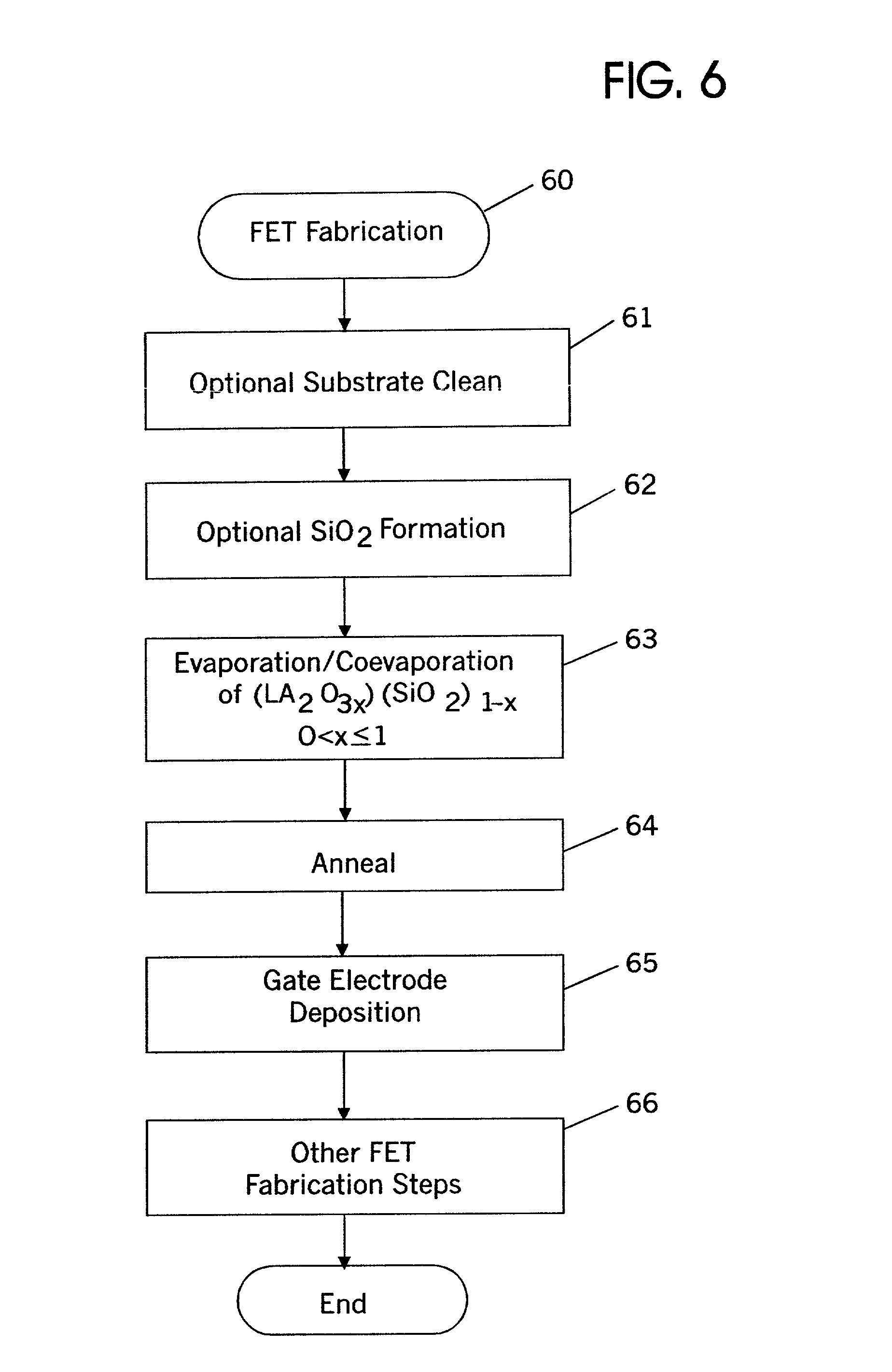
[0055] Dielectric layers according to embodiments of the present invention were fabricated as was described in connection with FIG. 6. X-ray diffraction patterns were collected. In general, diffraction data can be collected from dielectric layers as thin as 100 .ANG.. FIGS. 9A-9C illustrate diffraction patterns for 100 .ANG. samples. FIG. 9A illustrates an as-deposited sample (Block 63), FIG. 9B illustrates a sample annealed (Block 64) at 900.degree. C., and FIG. 9C illustrates a sample annealed at 1000.degree. C. As can be seen from FIGS. 9A-9C, these samples appear to be crystallization resistant until about 900.degree. C., so that amorphous layers are provided.

[0056] A gate electrode may be patterned, for example using conventional lithography and liftoff (Block 65), to form capacitors. Capacitor sizes may range from 50 .mu.m to 400 .mu.m squares, and may be within 1% of th...


PUM


Abstract

Lanthanum oxide-based gate dielectrics are provided for integrated circuit field effect transistors. The gate dielectrics may include lanthanum oxide, preferably amorphous lanthanum oxide and/or an alloy of lanthanum oxide and silicon oxide, such as lanthanum silicate (La.sub.2SiO.sub.5). Lanthanum oxide-based gate dielectrics may be fabricated by evaporating lanthanum on a silicon surface of an integrated circuit substrate. The lanthanum may be evaporated in the presence of oxygen. Lanthanum and silicon may be co-evaporated. An anneal then may be performed. Lanthanum oxide-based dielectrics also may be used for integrated circuit capacitors.

Description

FIELD OF THE INVENTION[0001] This invention relates to integrated circuit field effect transistors and fabricating methods therefor, and more particularly to gate dielectrics for integrated circuit field effect transistors and fabricating methods therefor.BACKGROUND OF THE INVENTION[0002] Integrated circuit Field Effect Transistors (FETs) are widely used in microprocessor, logic, memory and / or other integrated circuit devices. As is well known to those having skill in the art, an Insulated Gate integrated circuit Field Effect Transistor (IGFET), often referred to as a Metal Oxide Semiconductor (MOS) device or MOSFET device, includes spaced apart source and drain regions in an integrated circuit substrate and an insulated gate on the integrated circuit substrate therebetween, wherein the insulated gate includes a gate dielectric on the integrated circuit substrate and a gate electrode on the gate dielectric opposite the integrated circuit substrate. Complementary (n-channel and p-cha...

Claims


Application Information

Patent Timeline
Patent Type & Authority Applications(United States)
IPC IPC(8): H01L21/02H01L21/28H01L21/316H01L21/8242H01L29/51
CPCH01L21/28185H01L21/28194H01L21/28238H01L21/31604H01L27/10873H01L28/56H01L29/513H01L29/517H01L21/02156H01L21/02269H01L21/02192H01L21/0214H01L21/02238H01L21/02274H01L21/02255H10B12/05
Inventor MARIA, JON-PAULKINGON, ANGUS IAN
Owner NORTH CAROLINA STATE UNIV
Why Eureka
Try Eureka