Method and apparatus for manufacturing image displaying apparatus

a technology of image displaying apparatus and manufacturing method, which is applied in the manufacture of discharge tube main electrodes, electrode systems, electric discharge tube/lamps, etc., and can solve the problems of vacuum exhaustion of each vacuum chamber, inconvenient use, and long time-consuming

Inactive Publication Date: 2001-11-15
CANON KK
View PDF12 Cites 14 Cited by
  • Summary
  • Abstract
  • Description
  • Claims
  • Application Information

AI Technical Summary

Problems solved by technology

The manufacturing method according to the conventional art described above requires considerably long time for manufacturing one display panel, thus is not suitable for manufacturing a display panel inside of which requires the vacuum degree of 10-6 Pa or more.
Also, the second manufacturing method includes a problem in that it takes a long period of time for exhausting a gas from the space within the panels of the image displaying apparatus, and for introducing a gas containing an organic substance into the space with the panel.
In addition, since movement between each vacuum chamber of the FP and the RP is performed with breaking the atmosphere, each vacuum chamber is vacuum exhausted every time an FP and an RP are carried in.
As a result, the manufacturing process time becomes longer.

Method used


Image

  • Method and apparatus for manufacturing image displaying apparatus
  • Method and apparatus for manufacturing image displaying apparatus
  • Method and apparatus for manufacturing image displaying apparatus

Examples


second embodiment

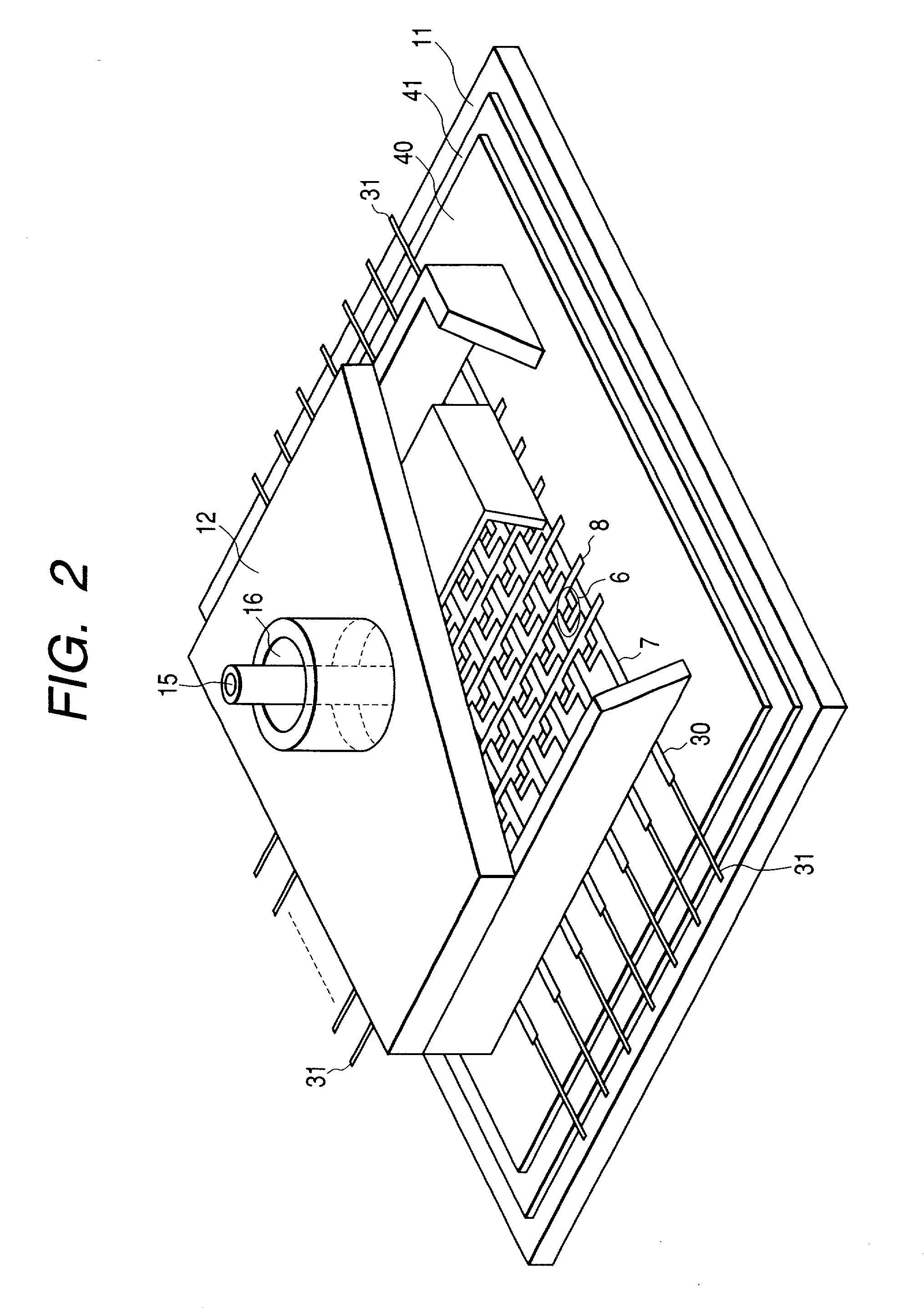
[0145] FIGS. 4 and 5 show a preferred second embodiment mode of the present invention. In FIGS. 4 and 5, reference numeral 14 denotes an auxiliary vacuum container, and reference numeral 17 denotes a gas exhausting path of the auxiliary vacuum container 14. The same members and the same parts as that in FIGS. 1 and 3 are shown by the same reference numerals.

first embodiment

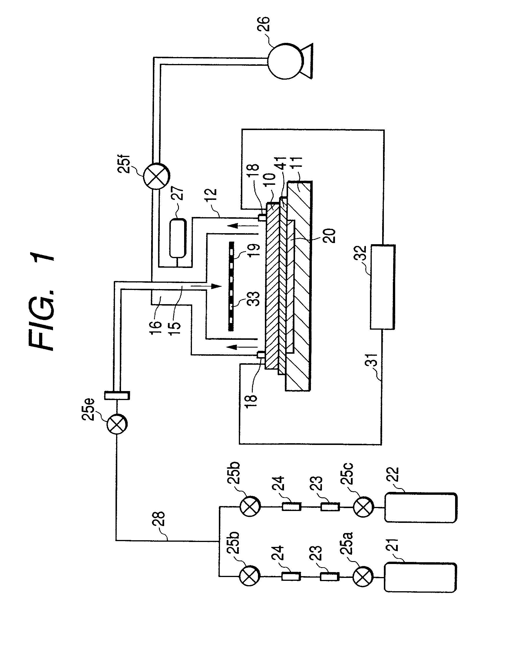
[0146] In the first embodiment mode, in the case that the size of the electron source substrate 10 is large, in order to prevent the electron source substrate 10 from breaking by the pressure difference between the front surface side and the back surface side of the diffusion plate 19, namely, the pressure difference between the pressure inside the vacuum container 12 and the atmospheric pressure, it is necessary to take a measure such as making the electron source substrate 10 into a thickness which can withstand the pressure difference, or relaxing the pressure difference by using a vacuum chucking mechanism as an electron source substrate fixing holding mechanism.

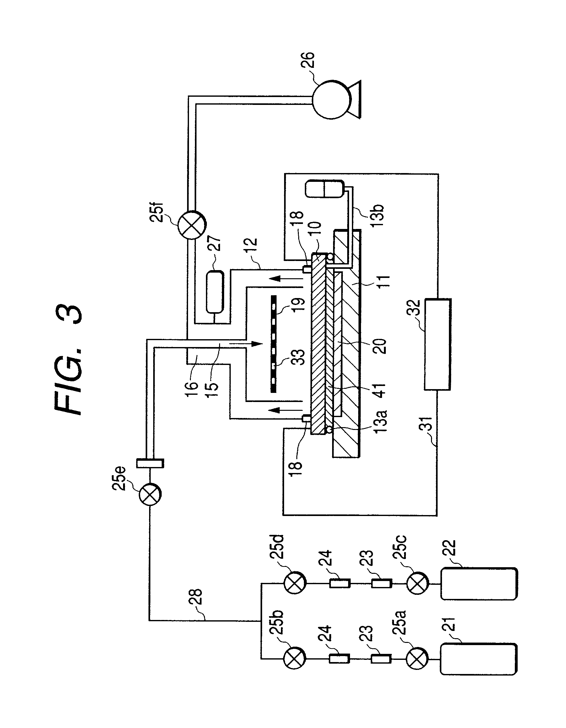
[0147] The second embodiment mode is an example that keeps in mind eliminating the pressure difference or making it small so as not to be a problem when sandwiching the electron substrate 10. In the second embodiment mode, the thickness of the electron source substrate 10 can be made thin, and in the case where the elect...

third embodiment

[0155] Next, a third embodiment mode of the present invention will be described by referring to FIG. 14. In this embodiment mode, in order to prevent the deformation or the damage of the electron source substrate 10 due to the pressure difference of the front and back of the electron source substrate 10, as described above, the substrate holder 207 is provided with an electrostatic chuck 208. The fixture of the electron source substrate 10 by the electrostatic chuck 208 is performed by applying a voltage between the electrode 209 arranged in the electrostatic chuck 208 and the electron source substrate 10 to suck the electron source substrate 10 to the substrate holder 208 by electrostatic force.

[0156] In order for the electron source substrate 10 to hold the predetermined potential, there is formed a conductive film such as an ITO film on the back surface of the electron source substrate 10. Note that, for adsorption of the electron source substrate 10 by the electrostatic chuck me...


PUM


Abstract

A method and an apparatus of manufacturing an image displaying apparatus comprising an electron source substrate and a phosphor substrate. The electron source substrate is provided with an electron emitting element formed by covering with a container and by applying a voltage to an electronic conductor on the substrate. While, the phosphor substrate is provided with a phosphor thereon. The substrates are subjected to a getter processing and to a seal bonding process under a vacuum condition through a processing chamber, to complete an image forming apparatus. An improvement resides in miniaturizing and simplifying operation, and in greater manufacture speed and mass production.

Description

[0001] 1. Field of the Invention[0002] The present invention relates to a method of manufacturing an image displaying apparatus in which a plurality of electron sources are arranged, and to an apparatus for manufacturing the same.[0003] 2. Related Background Art[0004] Conventionally, an electron-emitting device is roughly divided into two known types, i.e., a thermal electron-emitting device and a cold-cathode electron-emitting device. The cold-cathode electron-emitting device includes a field emission type, a metal / insulating layer / metal type, a surface conduction electron-emitting device, and the like.[0005] A surface conduction electron-emitting device is to utilize such a phenomenon that electron emission generates by flowing electric current to a thin film with a small area formed on a substrate, in parallel with the surface of the film. The applicant of the present invention made a large number of proposals on the surface conduction electron-emitting device having a novel stru...

Claims


Application Information

Patent Timeline
Patent Type & Authority Applications(United States)
IPC IPC(8): H01J1/30H01J9/02H01J9/38
CPCH01J9/027H01J9/38H01J9/385H01J31/127H01J2201/3165H01J2209/385H01J2329/941H01J2329/945H01J1/30
Inventor NOMURA, ICHIRONAKATA, KOHEIKANEKO, TETSUYAMIYAZAKI, TOSHIHIKOSATO, YASUEOHNISHI, TOSHIKAZU
Owner CANON KK
Why Eureka
Try Eureka