

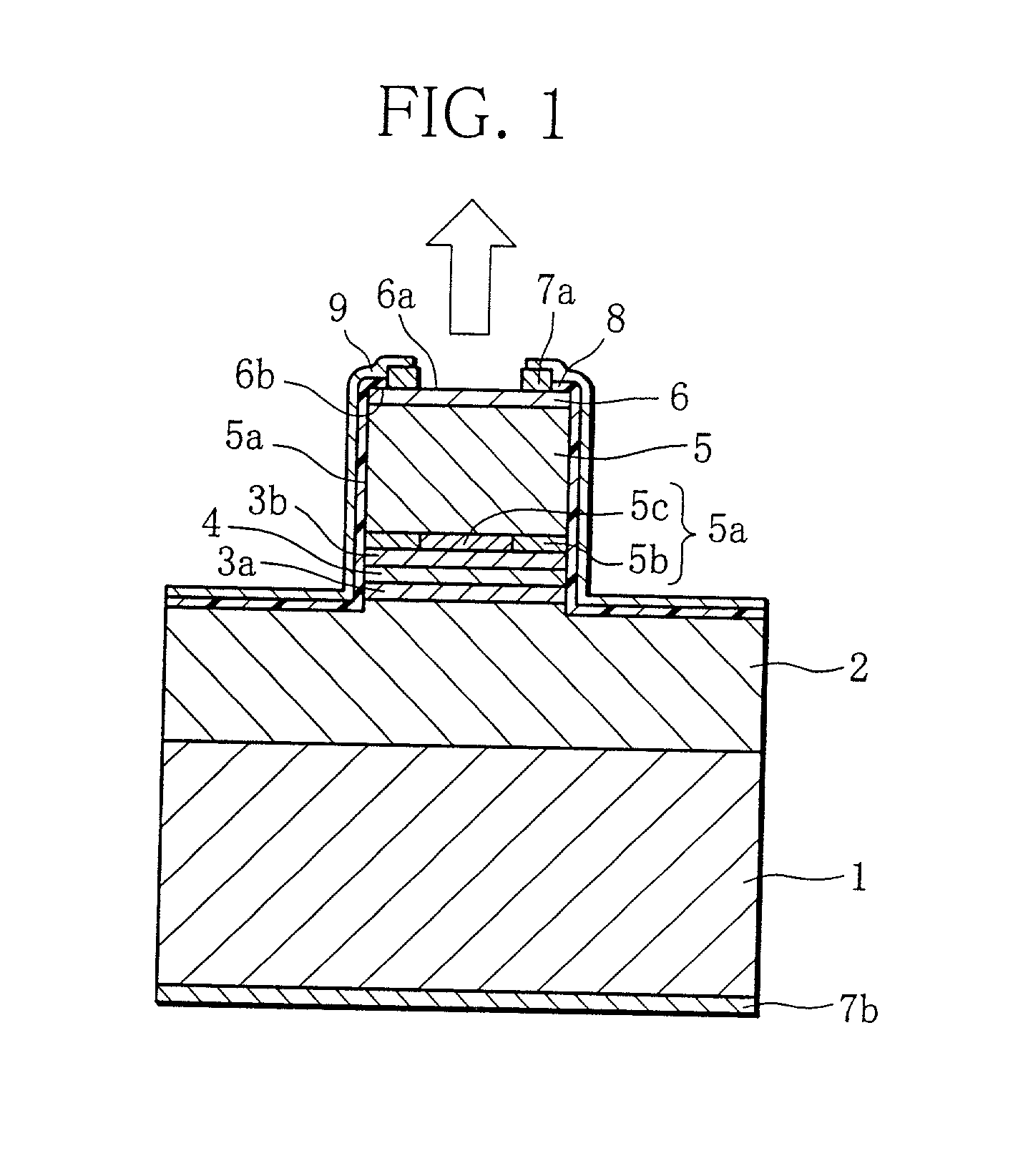
Surface emitting semiconductor laser device
a laser device and semiconductor technology, applied in semiconductor lasers, laser details, electrical equipment, etc., can solve the problems of high resistance of reflector layered structure, so as to achieve low resistance without causing the deterioration of optical output power characteristics of the laser devi
- Summary
- Abstract
- Description
- Claims
- Application Information
AI Technical Summary
Benefits of technology
Problems solved by technology
Method used
Image

Examples
Embodiment Construction
[0050] 1. Production of Laser Device
[0051] The laser device of the layered structure shown in FIGS. 2 and 3 was produced by the following steps.
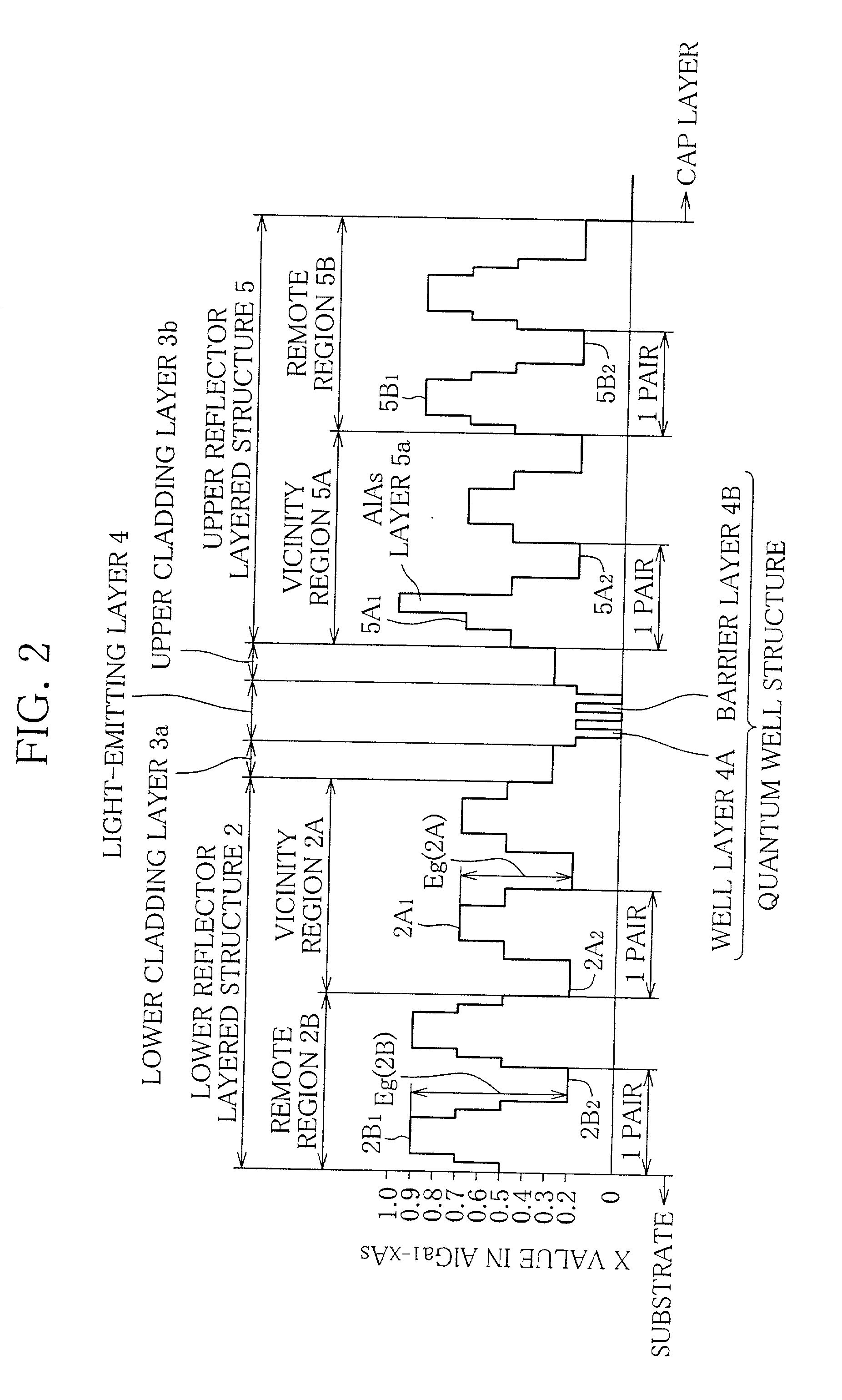
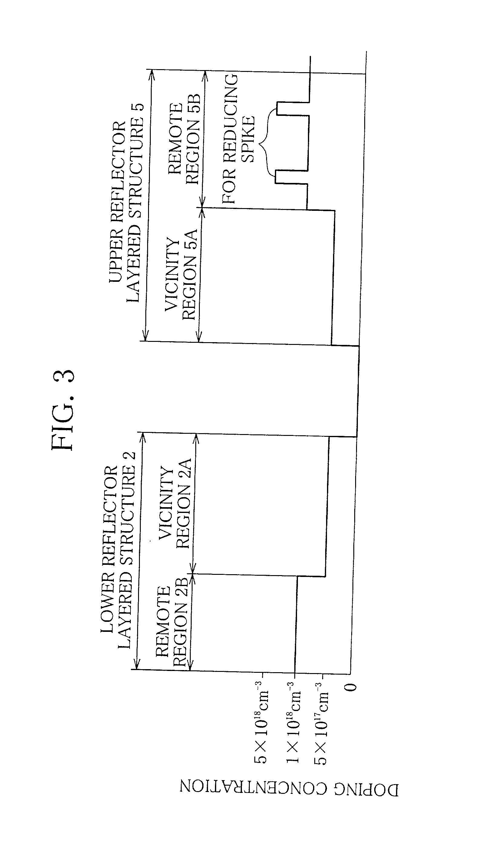
[0052] First, by an MOCVD process 30.5 paired layers, one pair layer (thickness: 111 nm) of which was formed by the hetero junction of Al.sub.0.9Ga.sub.0.1As (thickness: 48 nm) and Al.sub.0.2Ga.sub.0.8As (thickness: 43 nm), were laminated on the n-type GaAs substrate 1, and at the same time the remote region 2B having the doped concentration of 1.times.10.sup.18 cm.sup.-3 was formed using Si as the n-type impurity. Further, on the obtained structure 5.5 paired layers, one pair layer (thickness: 109 nm) of which was formed by the hetero junction of Al.sub.0.7Ga.sub.0.3As (thickness: 46 nm) and Al.sub.0.2Ga.sub.0.8As (thickness: 43 nm), were laminated, and at the same time the remote region 2A having the doped concentration of 5.times.10.sup.17 cm.sup.-3 was formed using Si as the n-type impurity so that the lower reflector layered structure 2...
PUM
 Abstract
Description
Claims
Application Information