Method, chemistry, and apparatus for high deposition rate solder electroplating on a microelectronic workpiece

a microelectronic workpiece and high deposition rate technology, applied in the direction of electrolytic processes, semiconductor devices, electrolysis components, etc., can solve the problems of low deposition rate of solder, risk of electrical shorts between solder bumps, and failure to significantly increase the deposition rate. achieve the effect of separating the plurality

Inactive Publication Date: 2002-01-03
SEMITOOL INC
View PDF0 Cites 4 Cited by
  • Summary
  • Abstract
  • Description
  • Claims
  • Application Information

AI Technical Summary

Benefits of technology

[0015] In accordance with one aspect of the present invention, the contact assembly comprises a plurality of contacts disposed to contact a peripheral edge of the surface of the workpiece. The plurality of contacts execute a wiping action against the surface of the workpiece as the workpiece is brought into engagement therewith. Further, the contact assembly includes a barrier disposed interior of the plurality of contacts that includes a member disposed to engage the surface of the workpiece to effectively isolate the plurality of contacts from the electroplating solution.

Problems solved by technology

Even with multiple etch cycles, the under bump metallurgy layer may be difficult to remove completely, creating the risk of electrical shorts between solder bumps.
Several technical problems are typically associated with electroplating of tin / lead solder on semiconductor wafers and other microelectronic workpieces.
One problem relates to the relatively low rate at which deposition of the solder takes place.
Attempts to significantly increase the deposition rate have heretofore proven unsuccessful.
Most such attempts are hindered by the fact that a significant amount of gas evolves during the electroplating process, particularly when traditional inert anodes are employed.
The resulting gas bubbles impair the proper formation of the solder bumps and other structures formed from the solder deposit.
Additionally, removal of the evolved gases can be problematic.
This non-uniform distribution of current across the wafer, in turn, causes non-uniform deposition of the plated solder material.
But such thieving techniques add to the complexity of electroplating equipment, and increase maintenance requirements.
Another problem with electroplating of wafers concerns efforts to prevent the electric contacts themselves from being plated during the electroplating process.
While it is possible to provide sealing mechanisms for discrete electrical contacts, such arrangements typically cover a significant area of the wafer surface, and can add complexity to the electrical contact design.
Electroplated solder may not adhere well to the exposed barrier layer material, and is therefore prone to peeling off in subsequent wafer processing steps.
Further, solder that is electroplated onto the barrier layer within the reactor may flake off during the electroplating process thereby adding particulate contaminants to the electroplating bath.
Such contaminants can adversely affect the overall electroplating process.
The specific solder to be electroplated can also complicate the electroplating process.
As a consequence, use of the typical plurality of electrical wafer contacts (for example, six, (6) discrete contacts) may not provide adequate uniformity of the plated metal layer on the wafer.
Beyond the contact related problems discussed above, there are also other problems associated with electroplating reactors for solder plating.
Still further, existing electroplating reactors are often difficult to maintain and / or reconfigure for different electroplating processes.

Method used


Image

  • Method, chemistry, and apparatus for high deposition rate solder electroplating on a microelectronic workpiece
  • Method, chemistry, and apparatus for high deposition rate solder electroplating on a microelectronic workpiece
  • Method, chemistry, and apparatus for high deposition rate solder electroplating on a microelectronic workpiece

Examples


Embodiment Construction

Back Solder Electroplating Reactor Components

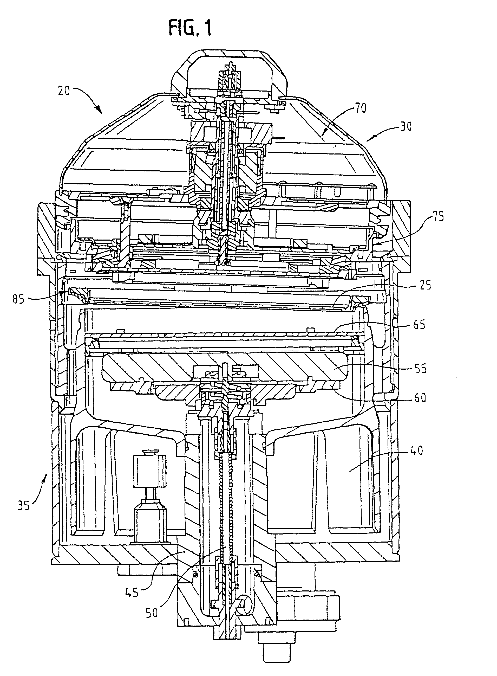
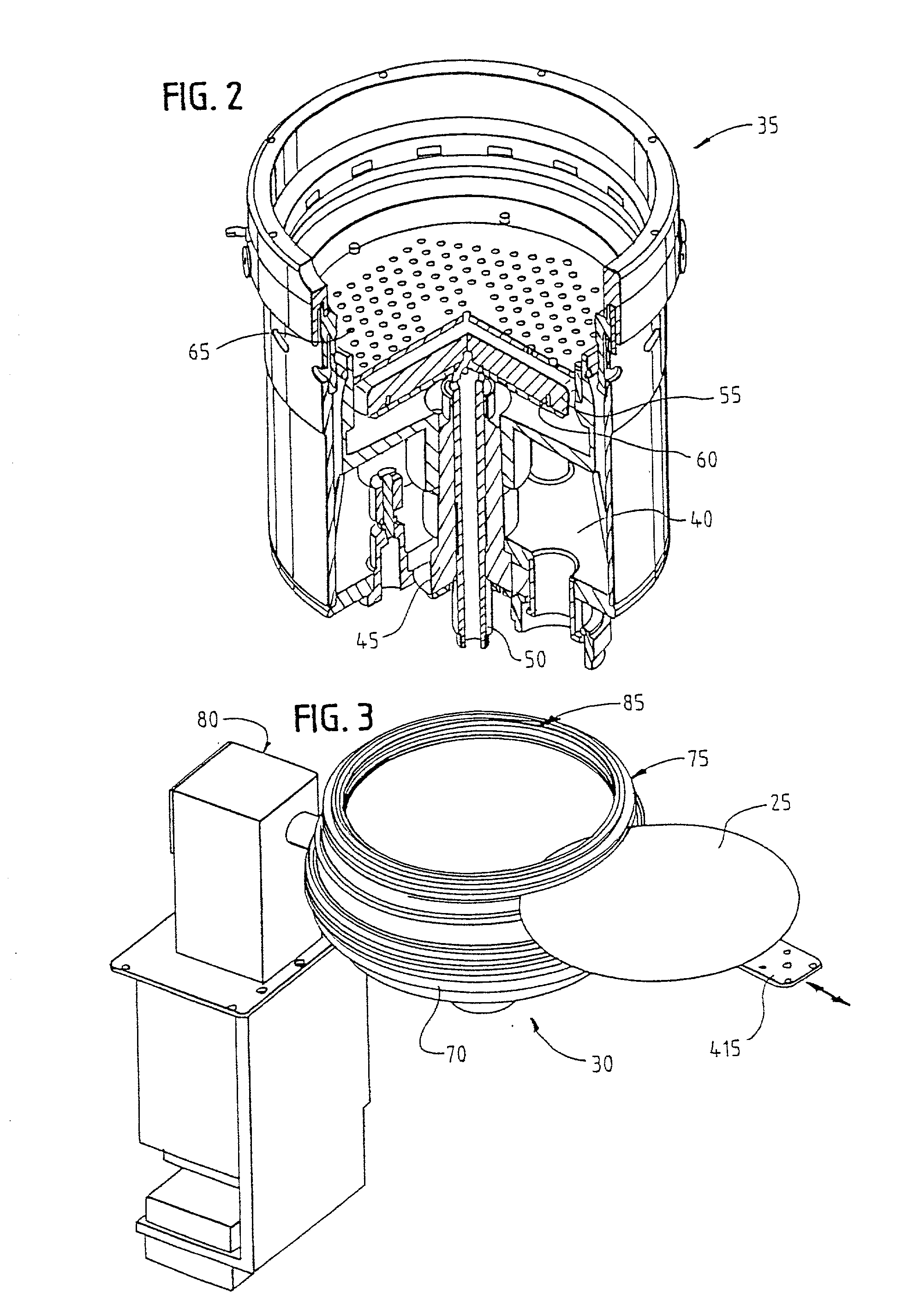
[0027] With reference to FIGS. 1-3, there is shown a reactor assembly 20 for high deposition rate electroplating of solder on a microelectronic workpiece, such as a semiconductor wafer 25. Generally stated, the reactor assembly 20 is comprised of a reactor head 30 and a corresponding reactor bowl 35. This type of reactor assembly is particularly suited for effecting electroplating of semiconductor wafers or like workpieces, in which an electrically conductive, thin-film seed layer of the wafer is electroplated with a blanket or patterned metallic layer, such as a layer of solder bumps.

[0028] The specific construction of one embodiment of a reactor bowl 35 suitable for use in the reactor assembly 20 is illustrated in FIG. 2. The electroplating reactor bowl 35 is that portion of the reactor assembly 20 that contains electroplating solution, and that directs the solution at a high flow rate against a generally downwardly facing surface of an...


PUM

PropertyMeasurementUnit
temperatureaaaaaaaaaa

Abstract

The present invention is directed to an improved electroplating method, chemistry, and apparatus for selectively depositing tin / lead solder bumps and other structures at a high deposition rate pursuant to manufacturing a microelectronic device from a workpiece, such as a semiconductor wafer. An apparatus for plating solder on a microelectronic workpiece in accordance with one aspect of the present invention comprises a reactor chamber containing an electroplating solution having free ions of tin and lead for plating onto the workpiece. A chemical delivery system is used to deliver the electroplating solution to the reactor chamber at a high flow rate. A workpiece support is used that includes a contact assembly for providing electroplating power to a surface at a side of the workpiece that is to be plated. The contact contacts the workpiece at a large plurality of discrete contact points that isolated from exposure to the electroplating solution. An anode, preferably a consumable anode, is spaced from the workpiece support within the reaction chamber and is in contact with the electroplating solution. In accordance with one embodiment the electroplating solution comprises a concentration of a lead compound, a concentration of a tin compound, water and methane sulfonic acid.

Description

[0001] Soldering has been a familiar technique for forming electrical and / or mechanical connections between metal surfaces and is the technique of choice for many applications in the electronics industry. Many soldering techniques have therefore been developed for applying solder to surfaces or interfaces between metals to extend soldering techniques to many diverse applications.[0002] In the electronics industry, in particular, the trend toward smaller sizes of components and higher integration densities of integrated circuits has necessitated techniques for application of solder to extremely small areas and in carefully controlled volumes to avoid solder bridging between conductors.[0003] High performance microelectronic devices often use solder balls or solder bumps for electrical interconnection to other microelectronic devices. For example, a very large scale integration (VLSI) chip may be electrically connected to a circuit board or other next level packaging substrate using s...

Claims


Application Information

Patent Timeline
Patent Type & Authority Applications(United States)
IPC IPC(8): C25D7/12
CPCC25D7/123C25D17/001C25D3/34C25D3/30
Inventor BATZ,, ROBERT W. JR.CONRADY, SCOTRITZDORF, THOMAS L.
Owner SEMITOOL INC
Why Eureka
Try Eureka