Method of manufacturing a gate in a semiconductor device

a manufacturing method and technology of semiconductor devices, applied in the direction of semiconductor devices, basic electric elements, electrical appliances, etc., can solve the problems of adversely affecting the operation of the device, the difficulty in and the difficulty in achieving the effect of reducing the thickness of the silicon oxide film to be formed

Inactive Publication Date: 2002-01-03
HYUNDAI ELECTRONICS IND CO LTD
View PDF0 Cites 66 Cited by
  • Summary
  • Abstract
  • Description
  • Claims
  • Application Information

AI Technical Summary

Problems solved by technology

As the design rule is reduced, however, it has become apparent that the thickness of the silicon oxide film to be formed cannot be reduced below the range of 25 .ANG. to 30 .ANG. because of a tunneling limit.
For example, in a design rule of 0.1, the thickness of the gate insulating film is expected to be in the range of 25 .ANG. to 30 .ANG.. Due to increase in an off-current by a direct tunneling, however, there is a possibility that it may adversely affect the operation of a device.
As the integration degree of a semiconductor device increases, however, when the thickness is formed in the range of 25 .ANG. to 30 .ANG., there is a possibility that its application is problematic because the value of the dielectric constant is lowered as the thickness is reduced.
However, in case where the gate is formed with a W / WN or W / TiN structure, if it is combined with an aluminum oxide film or a tantalum oxide film having an effective charge of -2 to 3.times.10.sup.12 / cm.sup.2-, because the work function of the gate ranges from 4.55 to 4.8 eV, there is a possibility that the following problem may occur.

Method used


Image

  • Method of manufacturing a gate in a semiconductor device
  • Method of manufacturing a gate in a semiconductor device

Examples


Embodiment Construction

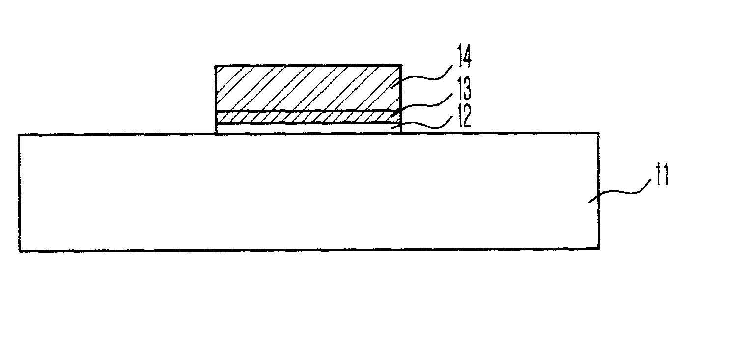
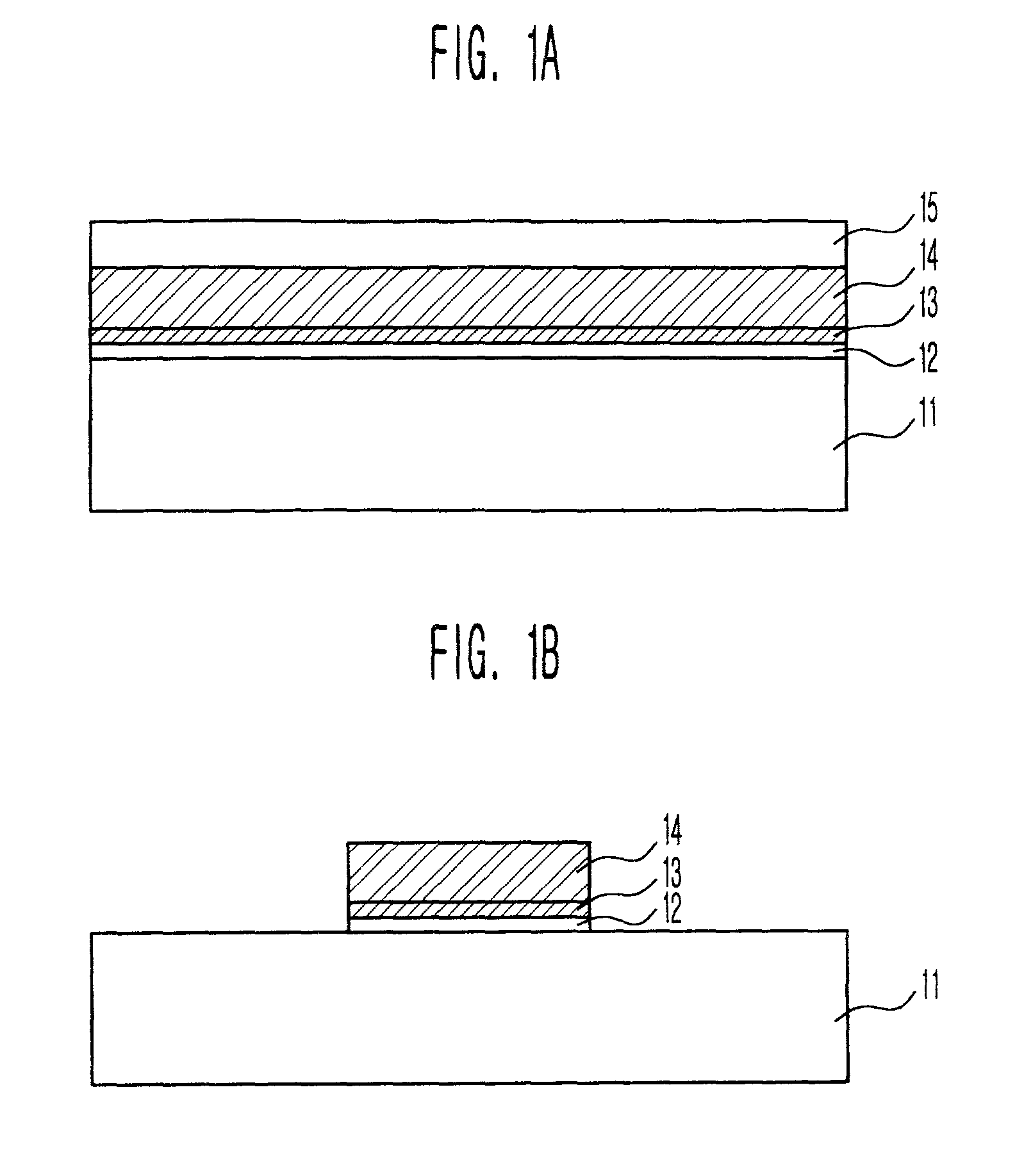
[0013] In the disclosed method, a TiAlN film as a barrier layer is formed between a gate insulting film and a metal gate. As the TiAlN film is formed by PVD method or CVD method, the work function of the TiAlN film is reduced compared to that of a TiN film. Therefore, a low threshold voltage can be obtained in a gate insulating film having a high dielectric constant such as Al.sub.2O.sub.3 or Ta.sub.2O.sub.5 having a negative effective charge. This employs the characteristic in which, in case of a TiAlN film having a solid solution characteristic of TiN and AlN, AlN having a wide band gap (.about.5 eV) and electron affinity ranging from about 1.5 to about 2 eV is added to form a barrier layer having a metal characteristic, and the work function at this time is reduced compared to that of TiN. Also, the TiAlN film has an advantage since it has a good oxidization-resistant compared to TiN.

[0014] The disclosed method will be described in detail by way of a preferred embodiment with ref...


PUM


Abstract

A method of manufacturing a gate in a semiconductor device is disclosed. The method forms a TiAlN film as a barrier layer between a gate insulating film and a metal gate by CVD method or PVD method resulting in the prevention of a leakage current and the obtaining of a low threshold voltage.

Description

[0001] 1. Field of the Invention[0002] The invention relates generally to a method of manufacturing a gate in a semiconductor device. More particularly, the invention relates to a method of manufacturing a gate in a semiconductor device, which can prevent a gate leakage current and obtain a low threshold voltage, by forming a TiAlN film between a gate insulating film and a metal gate.[0003] 2. Description of the Prior Art[0004] In the process of manufacturing DRAMs and logic devices, etc., which have been mass-produced, a silicon oxide (SiO.sub.2) film has been widely used as a gate insulating film. As the design rule is reduced, however, it has become apparent that the thickness of the silicon oxide film to be formed cannot be reduced below the range of 25 .ANG. to 30 .ANG. because of a tunneling limit. For example, in a design rule of 0.1, the thickness of the gate insulating film is expected to be in the range of 25 .ANG. to 30 .ANG.. Due to increase in an off-current by a direct...

Claims


Application Information

Patent Timeline
Patent Type & Authority Applications(United States)
IPC IPC(8): H01L21/28H01L21/316H01L29/423H01L21/336H01L29/43H01L29/49H01L29/51H01L29/78
CPCH01L21/28088H01L21/28202H01L21/28211H01L21/31604H01L21/31691H01L29/4966H01L29/513H01L29/517H01L29/518H01L21/18
Inventor PARK, DAE GYU
Owner HYUNDAI ELECTRONICS IND CO LTD
Why Eureka
Try Eureka