Simplified method of patterning field dielectric regions in a semiconductor device

a semiconductor device and simplified technology, applied in semiconductor/solid-state device manufacturing, basic electric elements, electric devices, etc., can solve the problems of increasing power consumption, increasing noise between devices, and increasing difficulty in maintaining performance and reliability, and achieve cost-effective

Inactive Publication Date: 2002-01-24
ADVANCED MICRO DEVICES INC
View PDF0 Cites 2 Cited by
  • Summary
  • Abstract
  • Description
  • Claims
  • Application Information

AI Technical Summary

Benefits of technology

[0017] An advantage of the present invention is an efficient cost-effective method of manufacturing a semiconductor device with accurately formed field dielectric regions.

Problems solved by technology

As device scaling plunges into the deep sub-micron ranges, it becomes increasingly difficult to maintain performance and reliability.
Isolation is important in the manufacture of integrated circuits which contain a plethora of devices in a single chip because improper isolation of transistors causes current leakage which, in turn, causes increased power consumption leading to increased noise between devices.
Accordingly, the evolution of integrated circuits is closely related to and limited by photolithographic capabilities.
There are, however, significant problems attendant upon the use of conventional LOCOS or STI methodology to form field dielectric regions in a semiconductor substrate.
For example, when a photoresist is coated on a highly reflective surface, such as silicon nitride which has an index of refraction of about 2.00, and exposed to monochromatic radiation, undesirable "swing effects" are produced as a result of interference between the reflected wave and the incoming radiation wave.
These swing effects cause the light intensity in the resist film to vary periodically as a function of resist thickness, thereby creating variations in the development rate along the edges of the resist and leading to uncontrolled line width variations.
These reflections make it difficult to control critical dimensions (CDs) such as linewidth and spacing of the photoresist and have a corresponding negative impact on the CD control of the shallow isolation trenches.
There are further disadvantages attendant upon the use of conventional LOCOS and STI methodologies.
For example, distortions in the photoresist are further created during passage of reflected light through the highly transparent silicon nitride layer which is typically used as a hardmask for STI etching.
Specifically, normal fluctuations in the thickness of the silicon nitride layer cause a wide range of varying reflectivity characteristics across the silicon nitride layer, further adversely affecting the ability to maintain tight CD control of the photoresist pattern and the resulting shallow isolation trenches.
Unfortunately, use of an ARC adds significant drawbacks with respect to process complexity.

Method used


Image

  • Simplified method of patterning field dielectric regions in a semiconductor device
  • Simplified method of patterning field dielectric regions in a semiconductor device
  • Simplified method of patterning field dielectric regions in a semiconductor device

Examples


Embodiment Construction

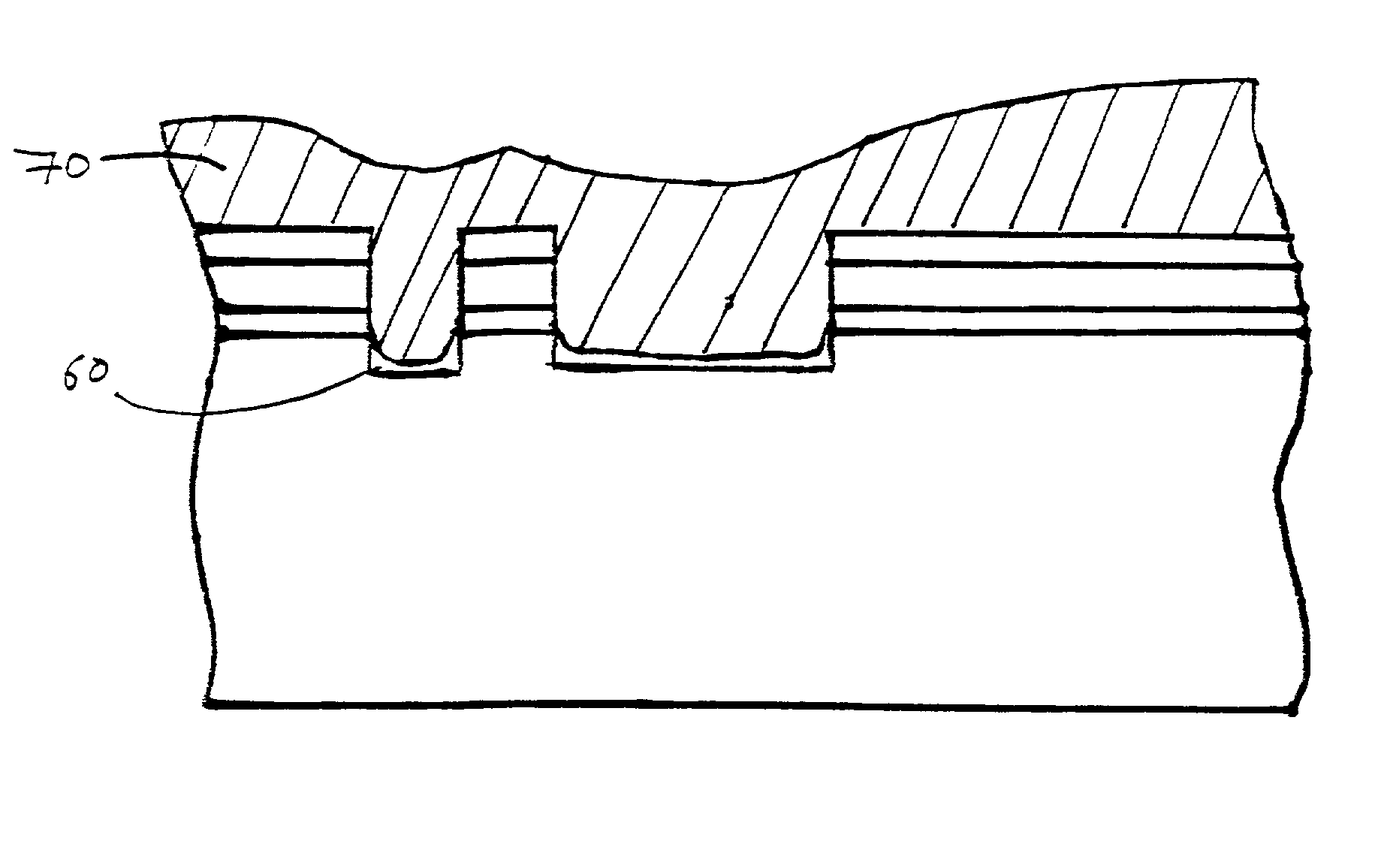
[0026] The present invention addresses and solves problems stemming from conventional methodologies of forming field dielectric regions, e.g., shallow trench isolations. Such problems include costly and time-consuming steps limited by materials which require different deposition systems and apparatus.

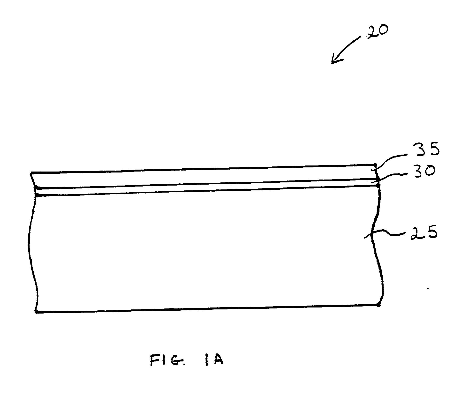
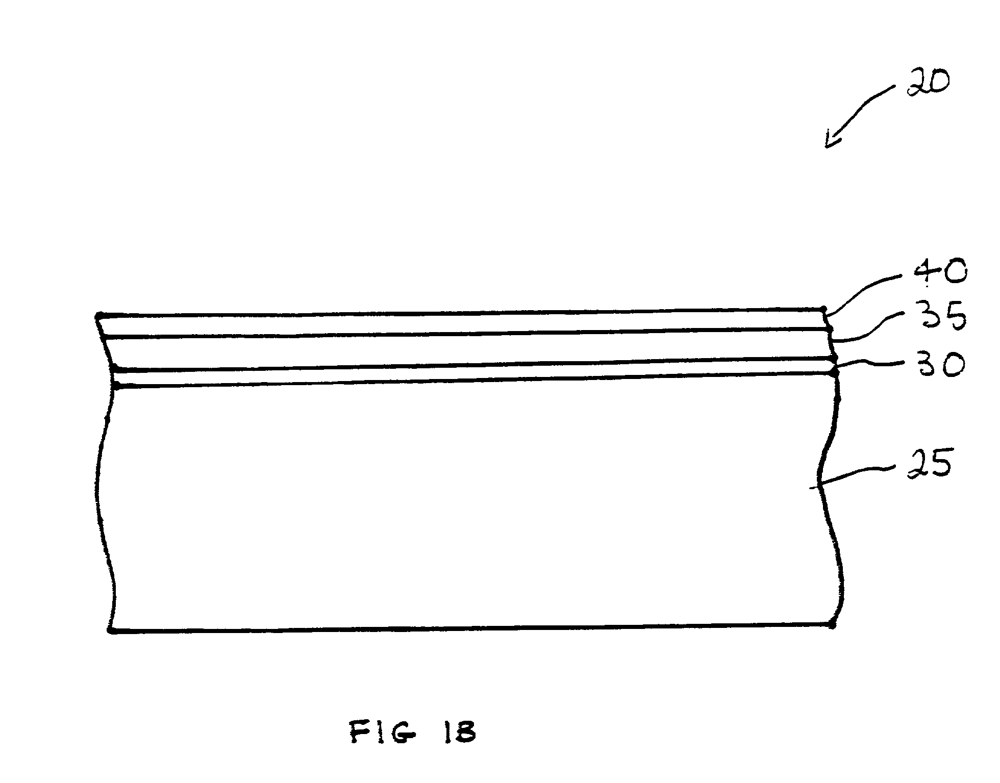
[0027] The present invention constitutes an improvement over conventional practices in forming field dielectric regions wherein a photoresist is deposited on a highly reflective surface, such as silicon nitride. The present invention enables the formation of dielectric regions with accurately controlled critical dimensions. In accordance with embodiments of the present invention, the semiconductor device can be formed by: forming an oxide layer on a semiconductor substrate; forming a silicon nitride layer on the oxide layer in a chamber; forming a silicon oxime coating on the silicon nitride layer in the chamber; and forming a photoresist mask on the silicon oxime coating. Embodiments o...


PUM

PropertyMeasurementUnit
thicknessaaaaaaaaaa
thicknessaaaaaaaaaa
thicknessaaaaaaaaaa

Abstract

Isolation regions are formed with greater accuracy and consistency by forming an oxide-silicon nitride stack and then depositing an antireflective layer, of silicon oxime, on the silicon nitride layer before patterning. Embodiments also include depositing the silicon nitride layer and the silicon oxime layer in the same tool.

Description

[0001] RELATED APPLICATIONS[0002] This application contains subject matter similar to subject matter disclosed in copending U.S. patent application Ser. No. ______, filed on ______, 1998 (our Docket No. 50100-947), and copending U.S. patent application Ser. No. ______, filed on ______, 1998 (our Docket No. 50100-948), and copending U.S. patent application Ser. No. ______, filed on ______, 1998 (our Docket No. 50100-949).[0003] The present invention relates to a method of manufacturing a semiconductor device having accurate and uniform field dielectric regions. The present invention is applicable to manufacturing high speed integrated circuits having submicron design features and high conductivity reliable interconnect structures.[0004] Current demands for high density and performance associated with ultra large scale integration require design rules of about 0.18 microns and under, increased transistor and circuit speeds and improved reliability. As device scaling plunges into the d...

Claims


Application Information

Patent Timeline
Patent Type & Authority Applications(United States)
IPC IPC(8): H01L21/762
CPCH01L21/76229
Inventor BHAKTA, JAYENDRA D.BABCOCK, CARL P.
Owner ADVANCED MICRO DEVICES INC
Why Eureka
Try Eureka