Self-aligned silicone process for low resistivity contacts to thin film silicon-on-insulator mosfets

a technology of silicon-on-insulator mosfets and self-aligning silicone, which is applied in the direction of semiconductors, electrical equipment, semiconductor devices, etc., can solve the problems of low parasitic resistance, low source/drain series resistance, and loss of silicide layer efficiency in reducing series resistan

Inactive Publication Date: 2002-03-14
INT BUSINESS MASCH CORP
View PDF16 Cites 19 Cited by
  • Summary
  • Abstract
  • Description
  • Claims
  • Application Information

AI Technical Summary

Benefits of technology

[0018] In this manner, a reaction of Co to initially form Co.sub.2Si, minimizes the silicon consumption of the thin SOI film. The consumption of the thin SOI film is additionally reduced by the deposition of a silicon or poly-silicon film on the Co.sub.2Si.
[0019] The present invention extends the use of a salicide-like process to thin SOI films, which are expected to be used in future SOI MOSFETs. Such thin-film SOI films will be advantageous in making the devices smaller, reducing the source / drain to substrate overlap capacitance, and eliminating the floating body voltage.

Problems solved by technology

However, using an ultra-thin SOI film can result in high source / drain series resistance.
Further, even if a conventional salicide was used with thin films, there is no guarantee of low parasitic resistance because an ultra-thin silicon film may be completely consumed during the silicide formation.
Alternatively, if the silicide layer is made extremely thin (e.g., less than 30 nm) to avoid consuming the thin SOI film, then the silicide layer loses its efficiency in reducing the series resistance.
A thinner silicide film may exhibit nucleation problems and some of the phases may not form.
All of this would lead to a very steep increase in the contact resistance.
The conventional salicide process is not applicable to the production of ultra-thin SOI MOSFETs, and therefore a new salicide process is required to overcome the problems of the conventional method.
Further, the conventional method and structures are deficient in their silicide / SOI interface roughness.

Method used


Image

  • Self-aligned silicone process for low resistivity contacts to thin film silicon-on-insulator mosfets
  • Self-aligned silicone process for low resistivity contacts to thin film silicon-on-insulator mosfets
  • Self-aligned silicone process for low resistivity contacts to thin film silicon-on-insulator mosfets

Examples


Embodiment Construction

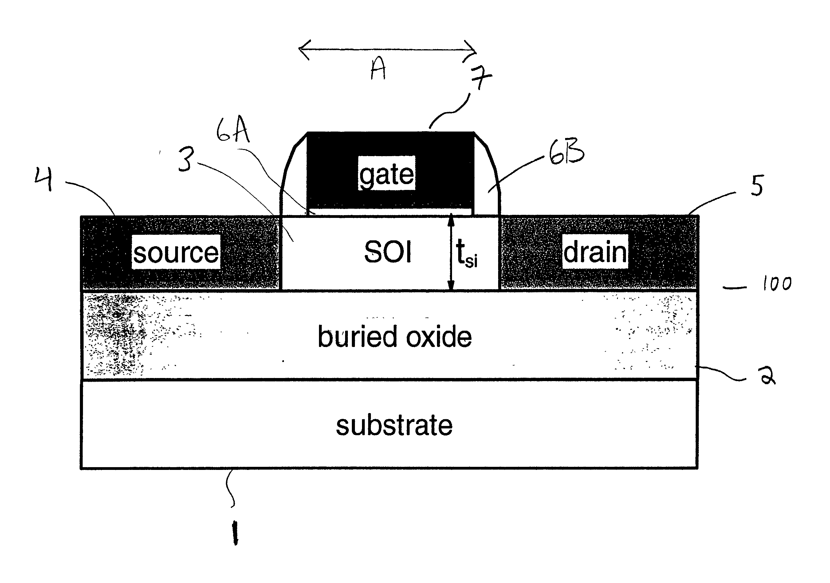
[0029] Referring now to the drawings, and more particularly to FIGS. 1-6, there is shown a preferred embodiment of the method of making of a self-aligned silicide which is applicable to the standard MOSFET structure, and also to non-conventional MOSFETs and structures according to the present invention.

[0030] Referring now to FIG. 1, a conventional MOSFET structure 100 is shown having a substrate 1 formed of silicon, a buried oxide layer 2 (e.g., silicon oxide layer), an SOI layer 3 which thickness noted by t.sub.si, a gate dielectric 6A (e.g., SiO.sub.2), sidewall spacers 6B formed of nitride or oxide, a gate 7 (e.g. doped poly-Si, or metal), and a source 4 and a drain 5 maid into the SOI film 3, typically by an implant.

[0031] The inventive method is directed to making a self-aligned silicide which is applicable to the standard MOSFET structure, and also to non-conventional MOSFETs and structures. For ease of discussion, the present invention will be applied to the conventional MOS...


PUM

PropertyMeasurementUnit
thicknessaaaaaaaaaa
thicknessaaaaaaaaaa
thicknessaaaaaaaaaa

Abstract

A silicide processing method for a thin film SOI device including depositing a metal or an alloy on a gate and a source / drain structure formed in a silicon-on-insulator film, reacting the metal or alloy at a first temperature with the silicon-on-insulator film to form a first alloy, etching the unreacted layer of the metal (or alloy) selectively, depositing a Si film on the first alloy, reacting the Si film at a second temperature to form a second alloy, and etching the unreacted layer of the Si film selectively.

Description

[0002] 1. Field of the Invention[0003] The present invention generally relates to silicon-on-insulator (SOI) MOSFETs and specifically, a self-aligned silicide (salicide) process for thin film SOI MOSFETs having low resistivity contacts.[0004] 2. Description of the Related Art[0005] Conventionally, a reduction of a short channel effect in a silicon-on-insulator (SOI) MOSFET has been addressed by using ultra-thin silicon films (e.g., having a thickness substantially within a range of about 50 nm to about 3 nm). However, using an ultra-thin SOI film can result in high source / drain series resistance. A portion of the high source / drain series resistance can be reduced by using a self-aligned silicide (salicide) contact (e.g., for a discussion of salicides, see Lisa T. Su et al., "Optimization of the series resistance in sub--0.2 .mu.m SOI MOSFET's", Electron Device Letters, 15(9), p. 363, September 1994).[0006] The conventional salicide process has been limited to bulk or thick SOI films...

Claims


Application Information

Patent Timeline
Patent Type & Authority Applications(United States)
IPC IPC(8): H01L21/28H01L21/285H01L21/336H01L29/45H01L29/49H01L29/786
CPCH01L21/28518H01L29/458H01L29/4908H01L29/665H01L29/66772H01L29/78
Inventor CABRAL, CYRIL JR.CHAN, KEVIN KOKCOHEN, GUY MOSHELAVOIE, CHRISTIANROY, RONNEN ANDREWSOLOMON, PAUL MICHAEL
Owner INT BUSINESS MASCH CORP
Why Eureka
Try Eureka