
Method for shifting the bandgap energy of a quantum well layer

a quantum well and bandgap energy technology, applied in the direction of lasers, nanooptics, laser details, etc., can solve the problems of severe damage in the quantum well structure, atoms in the sample vibrating violently, and points that can move around in the crystal structur

Inactive Publication Date: 2002-06-13
HO SENG TIONG
View PDF0 Cites 25 Cited by
  • Summary
  • Abstract
  • Description
  • Claims
  • Application Information

AI Technical Summary

Problems solved by technology

A point defect can move around in the crystal structure when the crystal structure is heated.
Heating can cause the atoms in the sample to vibrate violently.
The use of high-energy and / or high dose (i.e., a dose of greater than 1.times.10.sup.15 cm.sup.-2) ion implantation in conventional IID processes is known, however, to cause severe damage in the quantum well structure.
These drawbacks include difficulty in producing: (i) a low-loss waveguide photonic device due to free carrier absorption from implanted shallow-level ion species and scattering loss from complex defects induced by the IID process; (ii) photonic devices with controlled electrical characteristics (e.g., a desirable electrical conductivity or pn-junction properties) due to the aforementioned free carriers and complex defects, as well as due to re-distribution of dopants during the high temperature anneal step; and (iii) a photonic device with a high quality gain layer due to the IID process-induced complex defects, which create carrier recombination centers resulting in shorter carrier lifetime and lower optical gain.
The conventional ion implantation based IID processes do not adequately produce high quality photonic devices either in the form of single device or integrated multiple devices.
For example, conventional IID processes can achieve criteria (iii) and (iv), but have difficulty in satisfying criteria (i), (ii), (v) and (vi).
These vertical stress field lines tend to limit the diffusion of point defects horizontally, since it is hard for the point defects to move across the vertical stress field lines.
Deep-level species are not easy to ionize at room temperature and hence will not give rise to much free carriers in III-V semiconductor.
At this crystal site vacancy concentration, it is highly likely for crystal site vacancies to agglomerate together, thereby forming larger aggregates and undesirable complex defects.

Method used


Image

  • Method for shifting the bandgap energy of a quantum well layer
  • Method for shifting the bandgap energy of a quantum well layer
  • Method for shifting the bandgap energy of a quantum well layer

Examples


Embodiment Construction

[0051] Described herein are various exemplary processes and embodiments of the inventive TAIVID process. The processes can, for example, be used to monolithically integrate various photonic devices on the same substrate (e.g., a wafer), wherein the various photonic devices possess different quantum-well bandgap energies.

[0052] To be consistent throughout the present specification and for clear understanding of the present invention, the following definitions are hereby provided for terms used therein:

[0053] The term "deep-level ion species" refers to atomic species that are not ionized in III-V semiconductor materials at room temperature; and

[0054] The term "shallow-level ion species" refers to atomic species that become electrically active at room temperature.

[0055] The term "indirect-well implantation" refers to a process which utilizes an implantation condition for which the range of peak impurity and / or vacancy concentration is placed .gtoreq.0.5 .mu.m away from a quantum well s...


PUM


Abstract

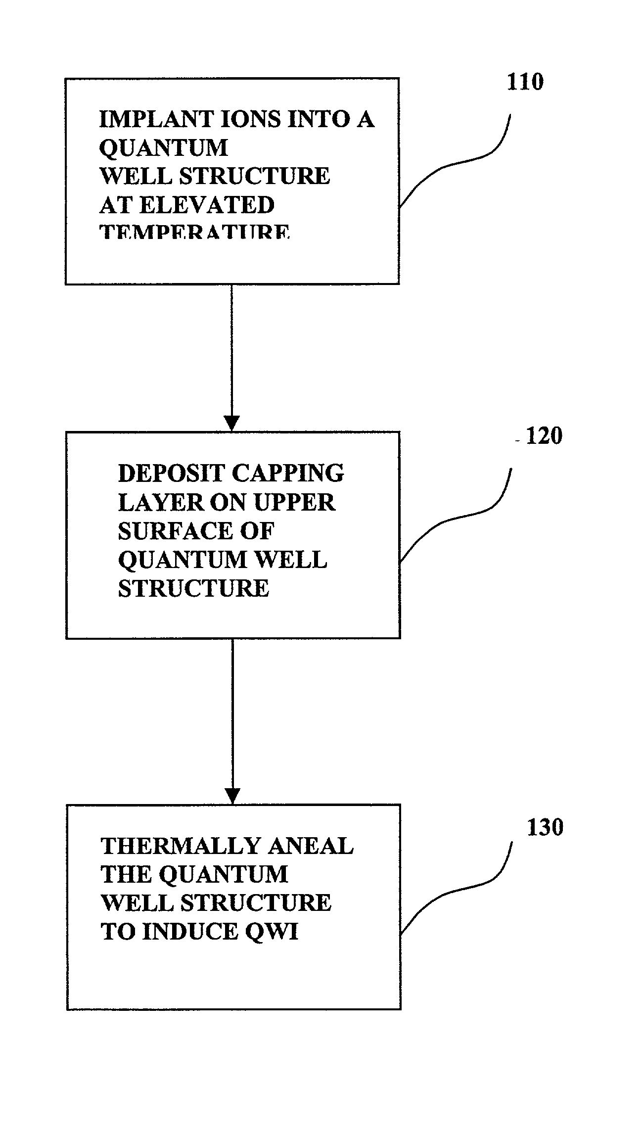
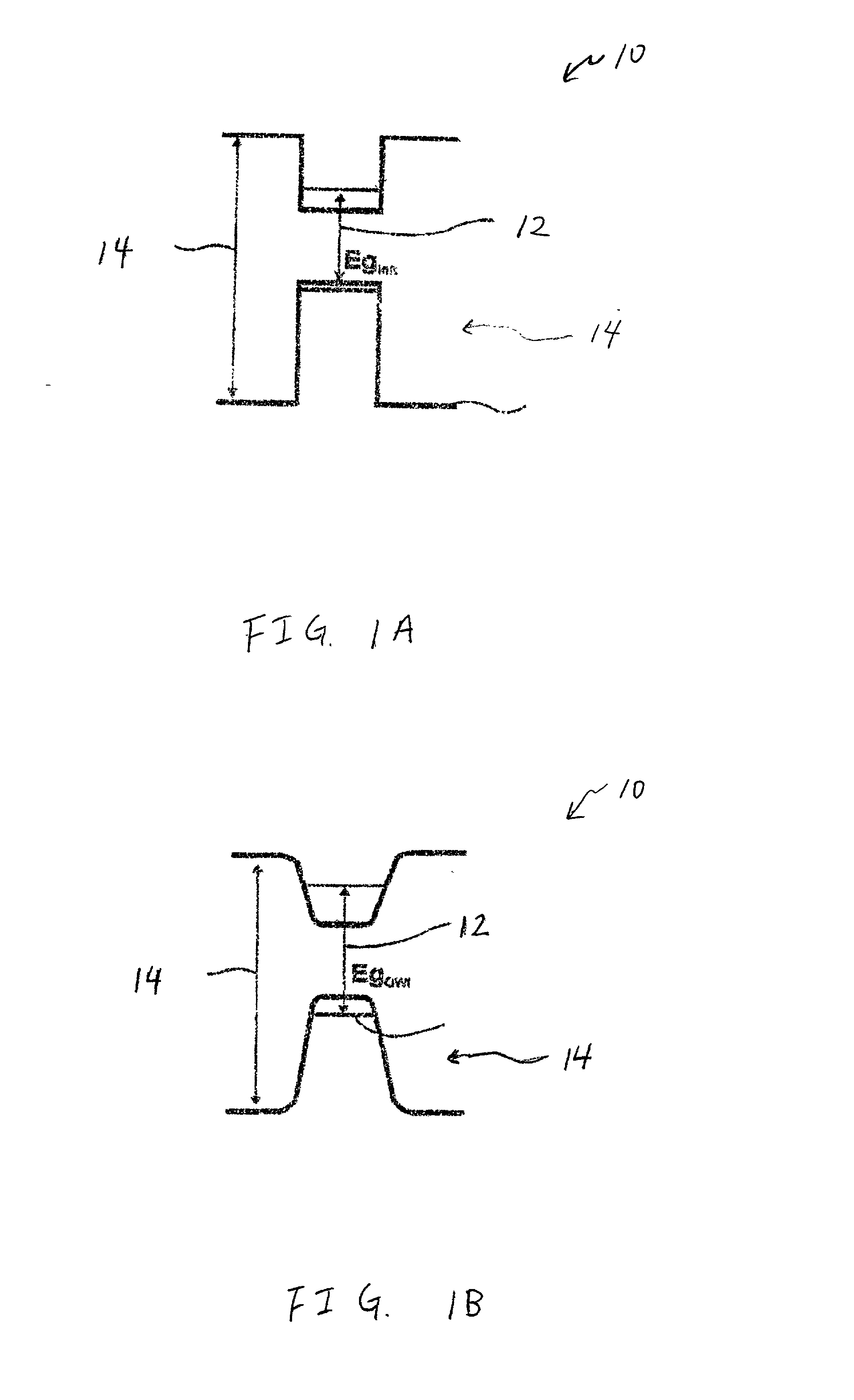
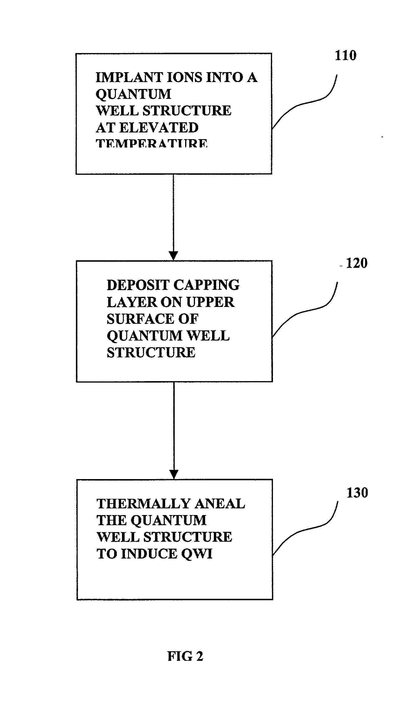
A process for shifting the bandgap energy of a quantum well layer (e.g., a III-V semiconductor quantum well layer) without inducing complex crystal defects or generating significant free carriers. The process includes introducing ions (e.g., deep-level ion species) into a quantum well structure at an elevated temperature, for example, in the range of from about 200 ° C. to about 700 ° C. The quantum well structure that has had ions introduced therein includes an upper barrier layer, a lower barrier layer and a quantum well layer. The quantum well layer is disposed between the upper barrier layer and the lower barrier layer. The quantum well structure is then thermally annealed, thereby inducing quantum well intermixing (QWI) in the quantum well structure and shifting the bandgap energy of the quantum well layer. Also, a photonic device assembly that includes a plurality of operably coupled photonic devices monolithically integrated on a single substrate using the process described above.

Description

CROSS-REFERENCES TO RELATED APPLICATIONS[0001] This application claims priority from U.S. provisional application No. 60 / 242,219, filed Oct. 20, 2000, which is hereby fully incorporated by reference.[0002] 1. Field of the Invention[0003] The present invention relates, in general, to photonic device manufacturing methods and, in particular, to methods for shifting the bandgap energy of quantum well layers and photonic devices and photonic integrated circuits formed thereby.[0004] 2. Description of the Related Art[0005] In the manufacturing of photonic devices, it is often desirable to employ processes that facilitate the monolithic integration of multiple photonic devices on a single substrate. This monolithic integration increases the yield, performance and functionality of the photonic devices and reduces manufacturing cost. The multiple photonic devices can include active photonic devices (e.g., lasers, optical intensity modulators, optical phase modulators, optical switches, opti...

Claims


Application Information

Patent Timeline
IPC IPC(8): H01L21/18H01S5/026H01S5/34
CPCB82Y20/00H01L21/182H01S5/026H01S5/3414H01S5/0265H01S5/3413H01S5/0261
Inventor OOI, BOON-SIEWHO, SENG-TIONG
Owner HO SENG TIONG
Learn More