Mask and projection exposure apparatus

a technology of masks and exposure apparatuses, which is applied in the direction of photomechanical apparatus, instruments, printing, etc., can solve the problems of affecting the quality of images, so as to achieve the effect of preventing or reducing the deterioration of image quality

Inactive Publication Date: 2002-07-04
CANON KK
View PDF5 Cites 22 Cited by
  • Summary
  • Abstract
  • Description
  • Claims
  • Application Information

AI Technical Summary

Benefits of technology

[0011] It is an object of the present invention to provide a mask and a projection exposure apparatus that may effectively prevent or decrease deterioration of image quality (quality of a circuit pattern image) based on a dustproof transparent member and / or circuit pattern writing errors.
[0019] The correction part may be formed such that a ray emits to a proper optical path from each portion in the pattern. The correction part may be formed such that a distortion of an image of the pattern is reduced when the image of the pattern is projected by a projection optical system in an exposure apparatus when the mask is installed into the exposure apparatus.
[0023] The projection exposure apparatus may further include a mechanism for adjusting a spherical aberration of the projection optical system. The adjusting mechanism may reduce a correction amount for a spherical aberration due to the transparent member.

Problems solved by technology

Therefore, it would become difficult to attain a high performance goal.
On the other hand, as the miniaturization advances, projection lenses with a higher performance than ever are needed, and the difficulty of the projection lens fabrication for the shortened exposure wavelength is drastically increasing.
However, a transparent member of such a plane parallel plate would flex because of its own weight when applied to an exposure apparatus, and a pattern (a circuit pattern image) projected by a projection optical system would include various aberrations, especially, a distortion, due to a transformation by transparent member's own weight.
On the other hand, if a circuit pattern written onto a mask plate is deviated from a design value of the circuit (or an ideal circuit pattern), it would result in a transfer of a distorted circuit onto the wafer.

Method used


Image

  • Mask and projection exposure apparatus
  • Mask and projection exposure apparatus
  • Mask and projection exposure apparatus

Examples


first embodiment

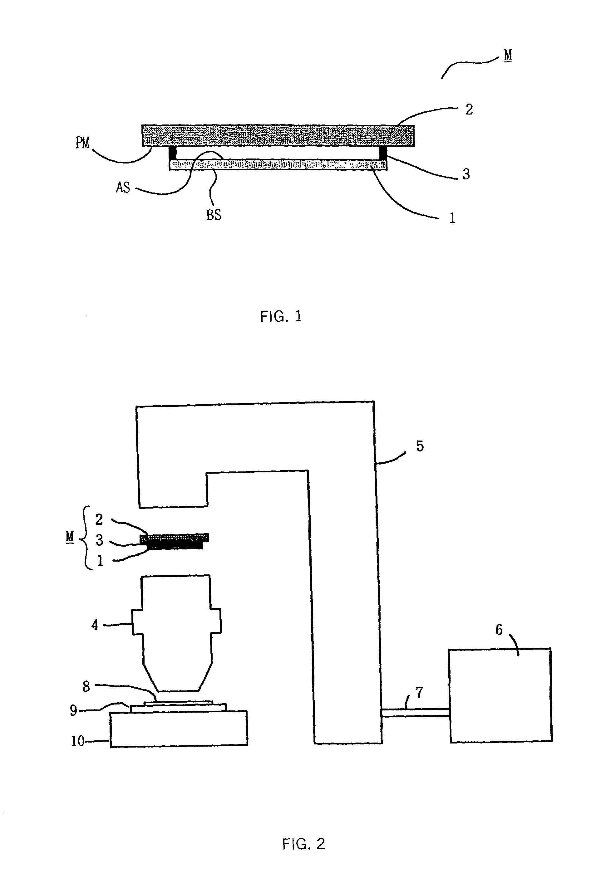
[0035] FIG. 1 shows a sectional view of main parts of a mask (also called a reticle) of the first embodiment according to the present invention.

[0036] In FIG. 1, the mask M includes members 1, 2, and 3. 2 denotes mask M's plate or base, and when it is incorporated into a projection exposure apparatus, a pattern (or a circuit pattern) is written on a surface at a side of the projection optical system (typically, bottom surface) PM. 1 denotes a dustproof transparent member (particle-proof member, i.e., pellicle) for preventing a foreign material from adhering to the pattern surface PM of the plate 2, and is supported by a supporting frame 3 attached to the mask plate 2 at a side of the (pattern) surface PM. The transparent member 1 and mask plate 2 are made of any glass material (including fluorine doped quartz and fluorite) transparent to light with a wavelength of 100-200 nm.

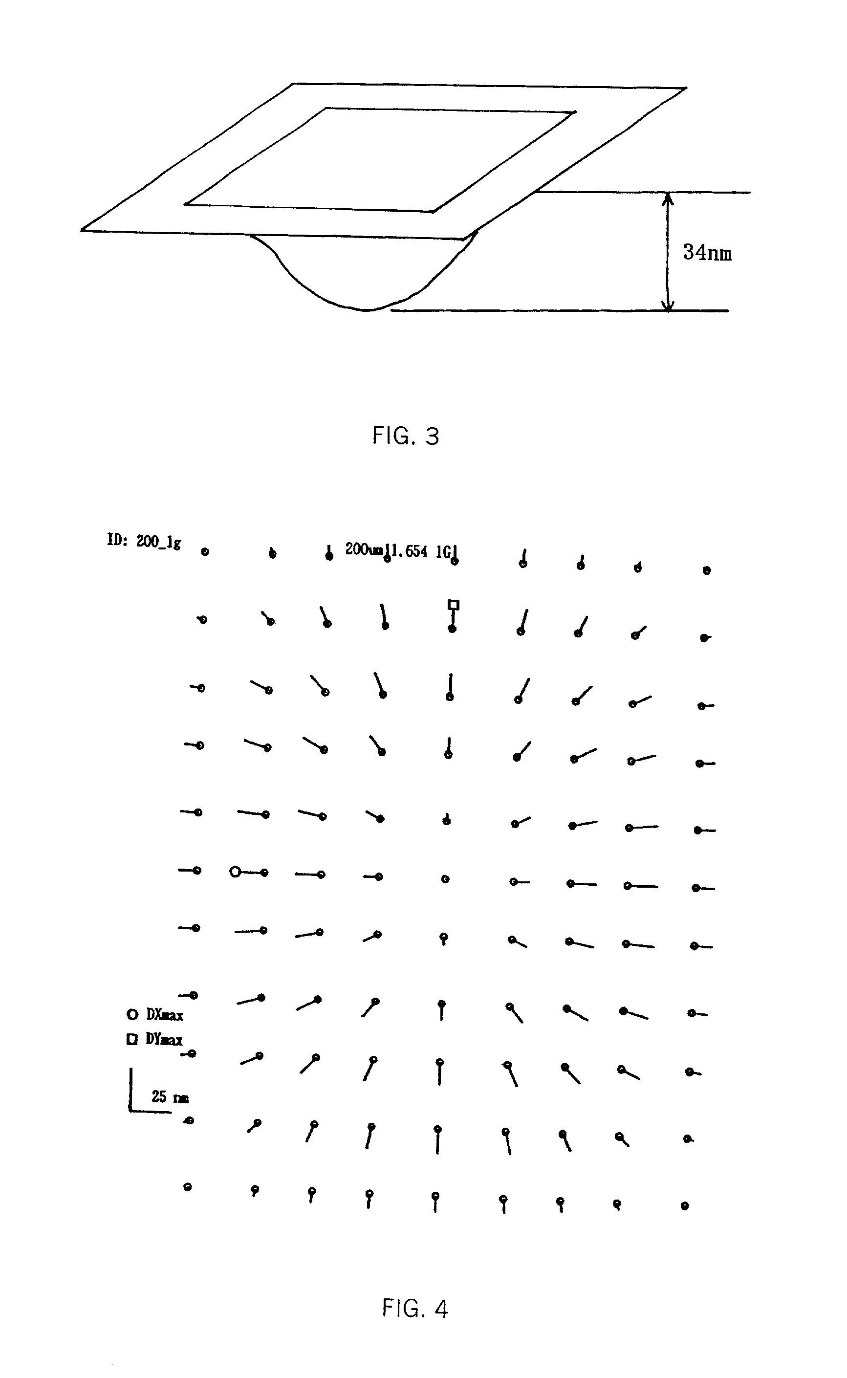
[0037] An aspheric surface is built on a surface AS at plate 2's side of the transparent member 1. The aspher...

second embodiment

[0041] FIG. 2 is a schematic view a projection exposure apparatus of the present invention.

[0042] According to the present embodiment, the present invention is applicable to a step-and-repeat and step-and-scan projection exposure apparatuses used in fabricating devices such as semiconductor devices, liquid crystal devices, imaging devices, magnetic heads, and the like.

[0043] A projection exposure apparatus in this embodiment includes a mask stage (not shown) for mounting various types of masks, an illumination optical system 5 for illuminating these masks, and an projection optical system 4, both the object and image sides of which are telecentric, for projecting a circuit pattern on the illuminated mask onto a wafer 8. The mask stage and each of the optical systems 4 and 5 are configured such that one of the masks M discussed in the first embodiment may be mounted and the circuit pattern on the mask M may be projected.

[0044] The illumination optical system 5 receives a laser beam w...

third embodiment

[0060] A description will now be given of a mask of the instant invention without reference to any drawing.

[0061] Compared to the mask in the first embodiment, the mask in the third embodiment mounts the dustproof transparent member directly onto the mask plate on which a pattern of an electronic circuit is written, without using the frame 3.

[0062] This reduces various aberrations due to the transformation of the transparent member by its own weight when the transparent member is applied to the projection exposure apparatus.

[0063] When a mask having no transparent member covering a pattern surface is mounted onto such a projection exposure apparatus for projection and exposure as uses a projection optical system designed and assembled for a mask having a transparent member covering a pattern surface, to project a pattern on the mask, an optical member that compensates for the thickness of the transparent member considered in the design may be inserted detachably in the optical path ...


PUM

PropertyMeasurementUnit
wavelengthaaaaaaaaaa
central wavelengthaaaaaaaaaa

Abstract

There is to provide a mask including a transparent member at a side of a surface of a base, a pattern being formed on the surface, and a correction part for correcting a change in an optical path of the transparent member.

Description

BACKGROUND OF THE INVENTION[0001] The present invention relates to masks and projection exposure apparatuses, in particular, those suitable for a photolithography process for fabricating various devices including semiconductor devices such as ICs and LSIs, image pick-up devices such as CCDs, display devices such as liquid crystal panels, and magnetic heads.[0002] A photolithography process for fabricating semiconductor devices uses a projection exposure apparatus to transfer a circuit pattern formed on a reticle or photo mask (called "a mask" hereinafter), onto a photosensitive material applied semiconductor wafer (or a photosensitive plate). Importantly, the projection exposure apparatus needs to use such a projection optical system as exhibits excellent image-forming performance with small aberration, so as to transfer the mask pattern onto the wafer under specified magnifications (reduction rate) with high accuracy. A recent demand on smaller semiconductor devices has accordingly...

Claims


Application Information

Patent Timeline
Patent Type & Authority Applications(United States)
IPC IPC(8): G02B13/22G02B13/24G03F1/62G03F7/20H01L21/027G02B13/14
CPCG03F1/62G03F1/72G03F7/70983G03F7/70308
Inventor KANDA, TSUNEO
Owner CANON KK
Why Eureka
Try Eureka