Pulsed laser deposition of transparent conducting thin films on flexible substrates

a technology of conducting thin films and flexible substrates, which is applied in the direction of photovoltaic energy generation, electrical equipment, semiconductor devices, etc., can solve the problems of damage to the surface of both the substrate and the film, and the sputtering technique cannot be used to grow the electrode film, etc., to achieve a smooth surface, lower electrical resistivity, and high optical transparency

Inactive Publication Date: 2002-07-25
THE UNITED STATES OF AMERICA AS REPRESENTED BY THE SECRETARY OF THE NAVY
View PDF0 Cites 25 Cited by
  • Summary
  • Abstract
  • Description
  • Claims
  • Application Information

AI Technical Summary

Benefits of technology

0007] According to the present invention, the foregoing and other objects are attained by providing TCO thin films on flexible substrates which exhibit a smooth surface, higher optical transparency and lower electrical resistivity and methods of making same.

Problems solved by technology

These high temperatures generally damage the surfaces of both the substrate and the film.
In this case the sputtering technique cannot be used to grow the electrode film because the energetic species (>100 eV) from the sputter target damage the organic layer.
However, glass substrates are unsuitable for certain applications such as electronic maps and portable computers.
Where flexibility or safety issues are important glass is very brittle and cannot be used since it cannot be easily deformed, or is too heavy, especially for large area displays.
The rough surface morphology and high resistivity of the sputter-deposited ITO films significantly degrade the performance of the OLED.
The current method of depositing TCO films on plastic substrates by sputtering produces a rough surface morphology and high resistivity, which degrades the performance of the OLED.

Method used


Image

  • Pulsed laser deposition of transparent conducting thin films on flexible substrates
  • Pulsed laser deposition of transparent conducting thin films on flexible substrates
  • Pulsed laser deposition of transparent conducting thin films on flexible substrates

Examples


example 2

[0031] OLEDs were constructed using the transparent conducting films deposited by pulsed laser deposition.

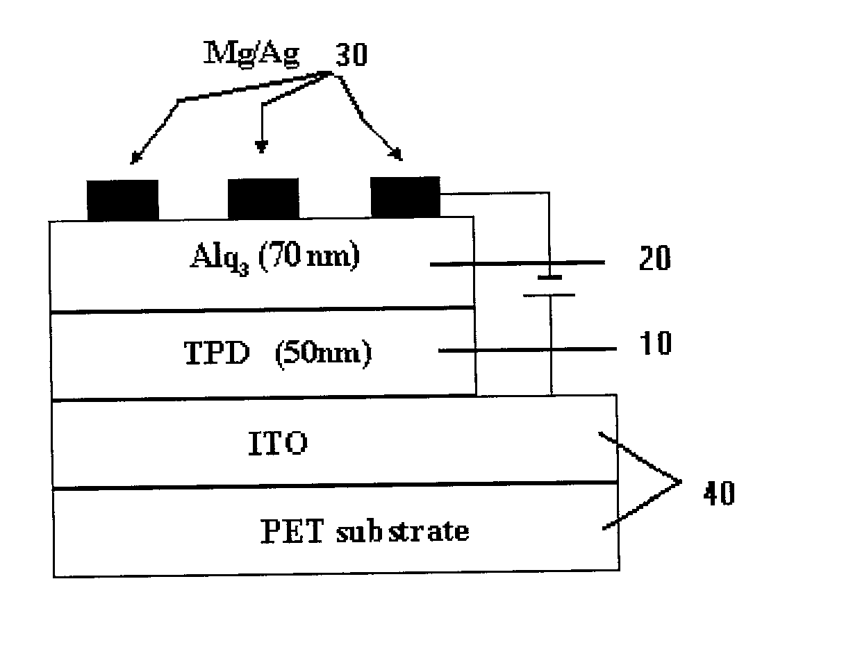
[0032] ITO thin films, deposited by PLD on PET substrates, were used as anode contacts in organic light-emitting diodes (OLEDs). The performance of the device was measured. FIG. 7(a) shows the OLED device configuration and FIG. 7(b) shows the chemical structures of the organic materials used in this research. The device structure consists of a hole transport layer (HTL) 10, of N, N'-diphenyl-N, N-bis (3-methylphenyl)1,1'-diphenyl-4,4'di-amine (TPD), 50, and an electron transport / emitting layer (ETL(EML) 20, of tris (8-hydroxyquinolinolato) aluminum (III) (Alq3), 60. The cathode contact 30, deposited on top of the ETL 20, is an alloy of Mg:Ag (ratio=12:1 by weight). Devices were fabricated by high vacuum vapor deposition, with a background pressure of 1.times.10.sup.-7 Torr. ITO coated substrates 40, were cleaned by an oxygen plasma asher. After the deposition of the organic laye...


PUM


Abstract

The invention relates to the deposition of transparent conducting thin films, such as transparent conducting oxides (TCO) such as tin doped indium oxide (ITO) and aluminum doped zinc oxide (AZO) on flexible substrates by pulsed laser deposition. The coated substrates are used to construct low cost, lightweight, flexible displays based on organic light emitting diodes (OLEDs).

Description

[0001] 1. Field of the Invention The invention relates generally to the deposition of transparent conducting thin films on flexible substrates by pulsed laser deposition (PLD), and more particularly to the deposition of thin films such as transparent conducting oxides (TCO) on flexible substrates.[0002] 2. Description of the Related Art[0003] Tin doped indium oxide (ITO) and aluminum doped zinc oxide (AZO) thin films, because they combine both transparent and conducting properties, have been widely used as transparent conducting electrodes in optoelectronic devices such as solar cells and flat panel displays (FPDs), surface heaters for automobile windows, camera lenses and mirrors, as well as transparent heat reflecting window material for buildings, lamps, and solar collectors. They are also widely utilized as the anode contact in organic light-emitting diodes (OLEDs). There are several deposition techniques used to grow these TCO films, including chemical vapor deposition (CVD), m...

Claims


Application Information

Patent Timeline
Patent Type & Authority Applications(United States)
IPC IPC(8): H01L31/18H01L51/00H01L51/30H01L51/52
CPCH01L31/1884H01L51/0059H01L51/0081H01L51/5206Y02E10/50H10K85/631H10K85/324H10K50/81
Inventor KIM, HEUNGSOOHORWITZ, JAMES S.KAFAFI, ZAKYA H.PIQUE, ALBERTOKUSHTO, GARY P.
Owner THE UNITED STATES OF AMERICA AS REPRESENTED BY THE SECRETARY OF THE NAVY
Why Eureka
Try Eureka