Method for forming dielectric stack without interfacial layer
a dielectric stack and interfacial layer technology, applied in the field of semiconductor device fabrication, can solve the problems of reducing the reliability of the sio.sub.2 layer as gate dielectric, limiting the capacitance, and posing the practical limit on the capacitance of a metal-oxide or silicate on the silicon structure, so as to increase the capacitance and reduce the leakage current
- Summary
- Abstract
- Description
- Claims
- Application Information
AI Technical Summary
Benefits of technology
Problems solved by technology
Method used
Image

Examples
Embodiment Construction
[0027] Detailed illustrative embodiments of the present invention are disclosed herein. However, specific structural and functional details disclosed herein are merely representative for purposes of describing preferred embodiments of the present invention.
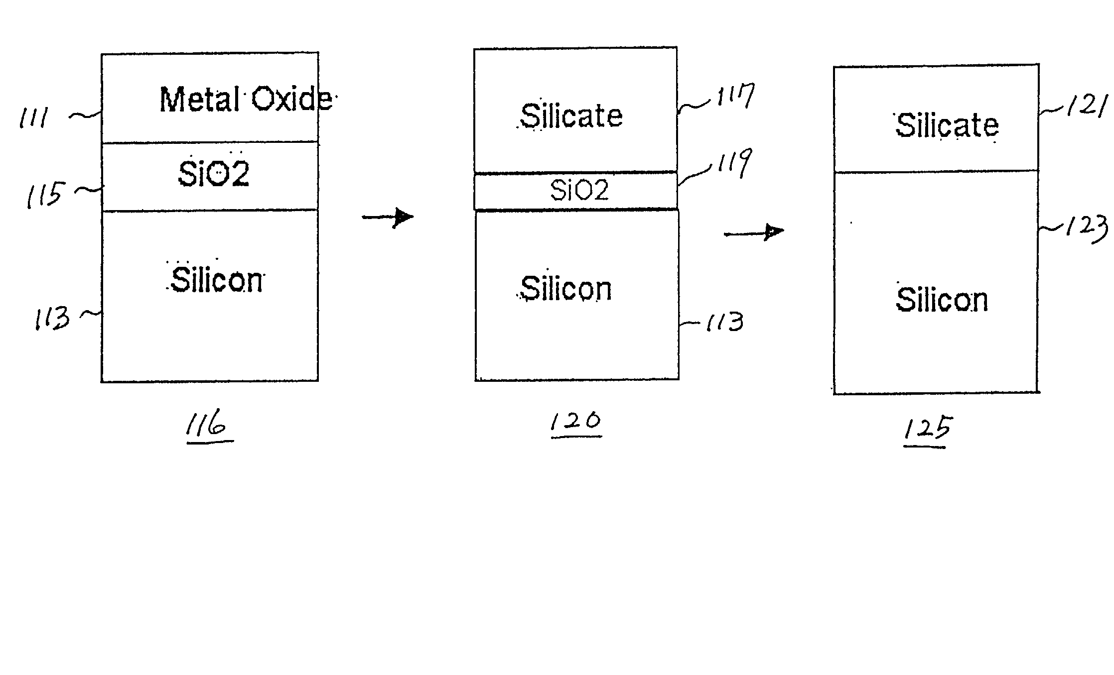
[0028] The present invention provides a method for forming a dielectric stack having substantially no interfacial silicon dioxide (SiO.sub.2) layer between a dielectric and a silicon substrate of the stack. The method of the present invention basically includes the processes of deposition of a metal-oxide on a silicon substrate and thermal processing of a metal-oxide based dielectric and a silicate based dielectric. The thermal processing has the effect of substantially removing an interfacial SiO.sub.2 layer formed between the dielectric and the silicon substrate.
[0029] Although, as mentioned above, the oxygen loss in most metal-oxides results in the destruction of the dielectric, the oxygen loss for certain metal-oxides and temp...
PUM
 Abstract
Description
Claims
Application Information
 - Generate Ideas
- Intellectual Property
- Life Sciences
- Materials
- Tech Scout
- Unparalleled Data Quality
- Higher Quality Content
- 60% Fewer Hallucinations
Browse by: Latest US Patents, China's latest patents, Technical Efficacy Thesaurus, Application Domain, Technology Topic, Popular Technical Reports.
© 2025 PatSnap. All rights reserved.Legal|Privacy policy|Modern Slavery Act Transparency Statement|Sitemap|About US| Contact US: help@patsnap.com