

Silicon-on-insulator(SOI)substrate
a technology of silicon-on-insulator and substrate, which is applied in the direction of semiconductor devices, semiconductor/solid-state device details, electrical devices, etc., can solve the problems of affecting the characteristics of crystal defects, affecting the performance of crystal defects, and affecting the quality of crystal defects
- Summary
- Abstract
- Description
- Claims
- Application Information
AI Technical Summary
Benefits of technology
Problems solved by technology
Method used
Image


Examples
example 2
[0099] In the second example, an SOI substrate was fabricated by a hydrogen ion separation process, using a silicon wafer, as the silicon substrate 1, which was fabricated by MCZ process and contained oxygen at a concentration of 5.times.10.sup.17 / cm.sup.3.
[0100] In the second example, there were prepared six different support substrates A to F, as follows.
[0101] 1. Support substrate A
[0102] The support substrate A has the same structure as the silicon substrate 1. That is, the support substrate A was a silicon wafer fabricated by MCZ process and containing oxygen at a concentration of 5.times.10.sup.17 / cm.sup.3.
[0103] 2. Support substrate B
[0104] The support substrate B was fabricated by applying heat treatment at 1000 degrees centigrade in O.sub.2 atmosphere to the support substrate A for thermal oxidation. Accordingly, the support substrate B was formed at a surface thereof with a 0.1 .mu.m-thick oxide film.
[0105] 3-6. Support substrates C-F
[0106] The support substrates C to F w...
second embodiment
[0117] Second Embodiment
[0118] In the second embodiment, a silicon wafer containing oxygen at a relatively high concentration is used as a silicon substrate after a region thereof close to a surface, at which an SOI active layer is to be formed, has been treated so as to reduce an oxygen concentration in the region. In the above-mentioned first embodiment, a silicon wafer containing oxygen at a relatively low concentration was used as the silicon substrate 1. However, an SOI active layer on which a device is to be fabricated occupies merely a part of a surface of a silicon substrate. Accordingly, if a region at which an SOI active layer is to be fabricated is designed to contain oxygen at a relatively low concentration, other region of the silicon substrate is allowed to contain oxygen at a relatively high concentration.
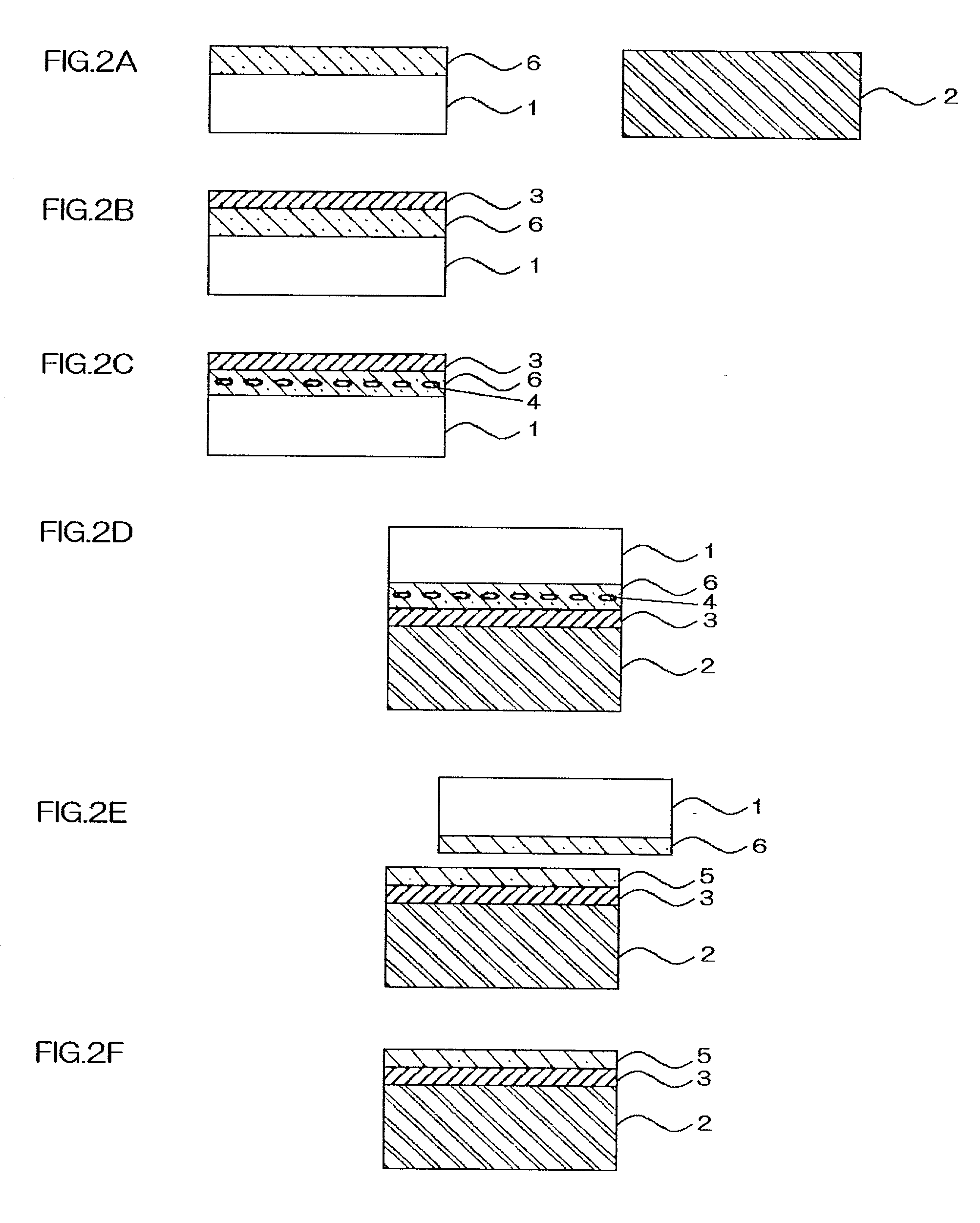
[0119] A method of fabricating an SOI substrate in accordance with the second embodiment is explained hereinbelow with reference to FIGS. 2A to 2F.
[0120] In the seco...
example 3
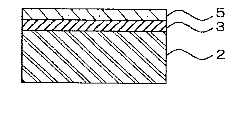
[0136] In the third example, there was used a silicon wafer fabricated by CZ process and containing oxygen at a concentration of as the silicon substrate 1. The silicon substrate 1 was formed at a surface thereof with the region 6 containing oxygen at a relatively low concentration. Then, an SOI substrate was fabricated by a hydrogen ion separation process.
[0137] The region 6 was formed by applying heat treatment in argon atmosphere to the silicon substrate 1 to thereby form a denuded zone. The heat treatment was carried out at 1200 degrees centigrade at atmospheric pressure in 100%-argon atmosphere for 5 hours. The thus formed region 6 had a depth of 10 .mu.m and contained oxygen at a concentration of 8.times.10.sup.17 / cm.sup.3.
[0138] In the third example, there were prepared four different support substrates A to D, as follows.
[0139] 1. Support substrate A
[0140] The support substrate A was a silicon wafer fabricated by CZ process and containing oxygen at a concentration of 2.times...
PUM
| Property | Measurement | Unit |
|---|---|---|
| temperature | aaaaa | aaaaa |
| temperature | aaaaa | aaaaa |
| temperature | aaaaa | aaaaa |
Abstract
Description
Claims
Application Information