Semiconductor device

Inactive Publication Date: 2002-12-05
SEIKO EPSON CORP
View PDF0 Cites 85 Cited by
  • Summary
  • Abstract
  • Description
  • Claims
  • Application Information

AI Technical Summary

Problems solved by technology

Flat MCPs in which the-semiconductor chips are lined up in a planar surface require a large mounting surface area, and hence contribute little to increasing the compactness of electronic equipment.
However, in the aforementioned semiconductor apparatus of Japanese Laid-Open Patent Publication 6-334098, assembly is complicated because the apparatus is produced joining the package main body 112, in which a cavity 115 is formed and printed boards having a set wiring pattern formed in advance are stacked up to one side of the flexible printed circuit board 116, creating the problem that the result effectively cannot be made compact.
In addition, with a conventional stacked MCP, it is necessary to form via holes and through holes for accomplishing inter-layer connection in order to electrically connect the semiconductor chips and the wiring board, and hence production processes, such as positioning between layers, processing holes, filling holes with a conductor or plating process, are difficult.
Consequently, the substrate is such that with the ridge folding lines, enlargement becomes necessary because of the fear that breaking of the wiring or the like could arise if the bending radius is

Method used


Image

  • Semiconductor device
  • Semiconductor device
  • Semiconductor device

Examples


first embodiment

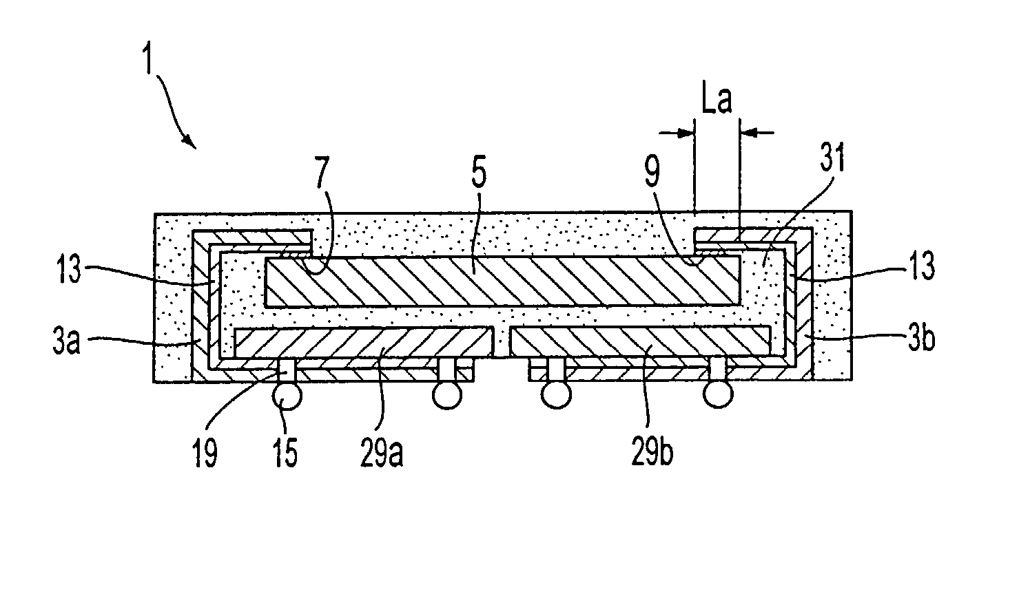
[0040] FIG. 1 is an open planar view of the semiconductor apparatus 1 according to the present invention, and FIG. 2 is a side cross-sectional view of the semiconductor apparatus 1.

[0041] In FIG. 1 or FIG. 2, with the semiconductor apparatus according to the first embodiment, a carrier tape material 3 is used which is rectangular with the long side in the sideways in the figure, and a semiconductor chip 5 (indicated by the broken line) is placed substantially in the center thereof, and interposers 29a and 29b are placed on both sides of this semiconductor chip 5, details of which are explained hereinafter. The semiconductor apparatus 1 is mounted such that the semiconductor chip 5 substantially in the center of the carrier tape material 3 is electrically connected. This semiconductor chip 5 is formed in the shape of a rectangle, and has a plurality of electrodes 7 and 9 in rows near the shorter opposing side in the narrow direction. These electrodes 7 and 9 are for example arranged ...

second embodiment

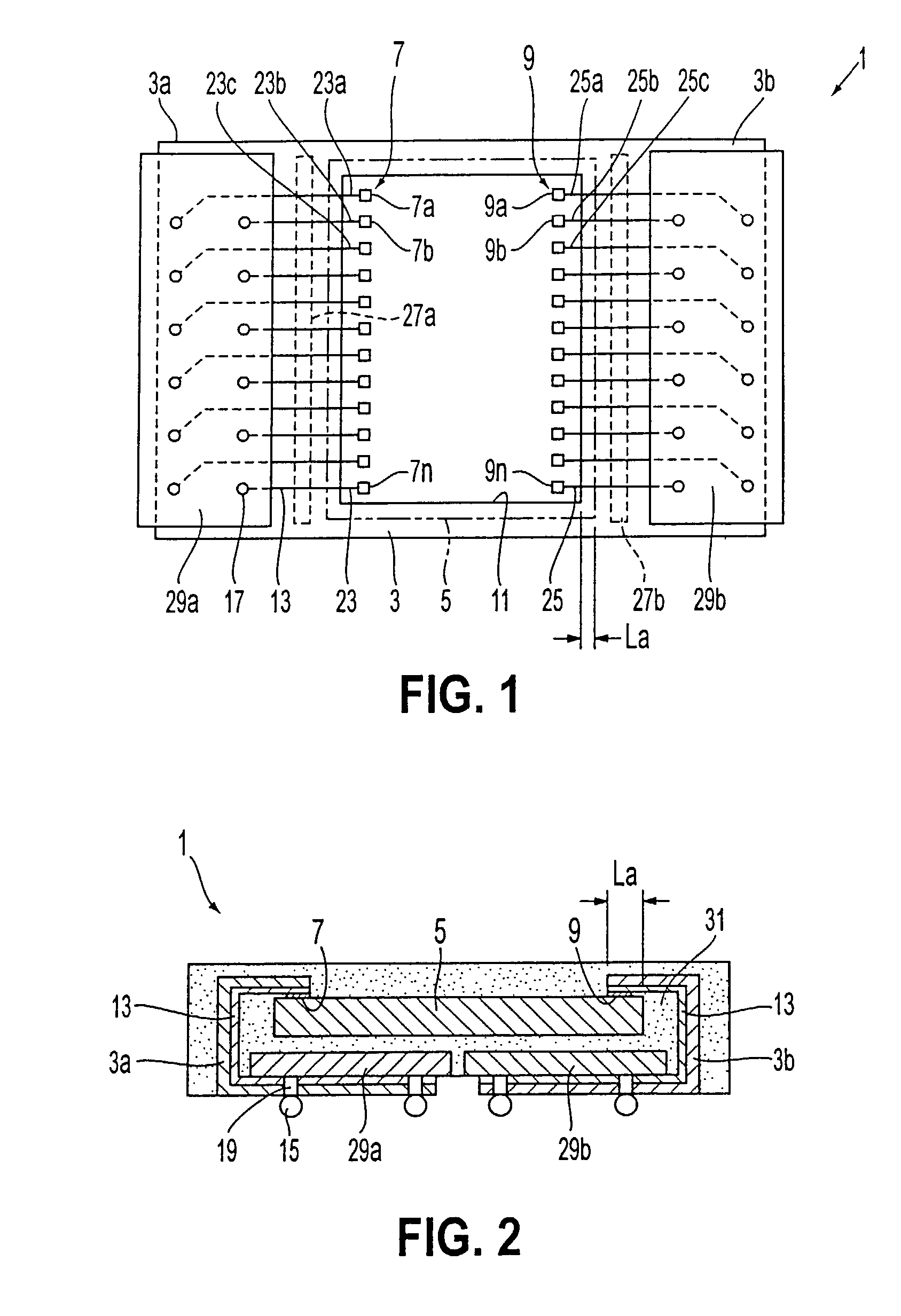
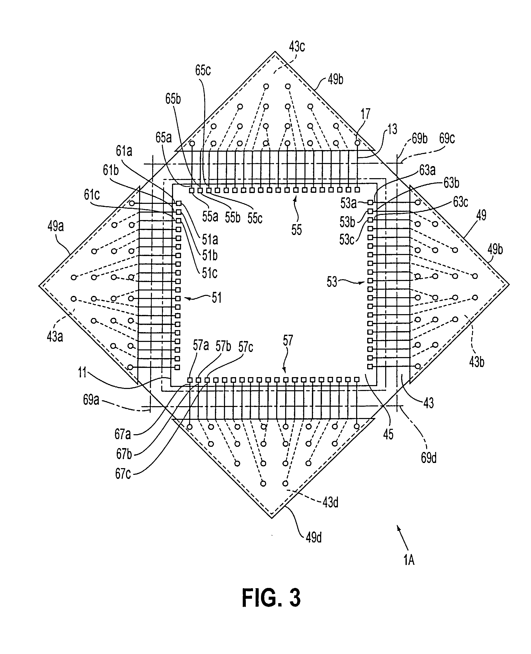
[0051] FIG. 3 is a planar view of a semiconductor apparatus 1A according to the present invention, FIG. 4 is a side cross-sectional view of the semiconductor apparatus 1A, and FIG. 5 is a post-assembly planar view of the semiconductor apparatus 1A.

[0052] In the semiconductor apparatus 1A of the second embodiment, a substantially square carrier tape material 43 is used, and a substantially square semiconductor chip 45 is positioned substantially in the center thereof, rotated by 90 degrees, and triangular interposers 49 protruding from the four edges of this semiconductor chip 45 are positioned so as to be freely bendable.

[0053] In FIG. 3 and FIG. 4, the semiconductor chip 45 is electrically connected and mounted substantially in the center of the carrier tape material 43. This semiconductor chip 45 is formed in a substantially square shape, and near each edge thereof has a plurality of electrodes 51, 53, 55 and 57. These electrodes 51, 53, 55 and 57 are arranged for example so that ...

third embodiment

[0064] FIG. 6 is a planar view of a semiconductor apparatus 1B according to the present invention, FIG. 7 is a cross-sectional view of the semiconductor apparatus 1B taken along line Y-Y in FIG. 1 and FIG. 8 is a cross-sectional view of the semiconductor apparatus 1B taken along line Z-Z in FIG. 1.

[0065] With the third embodiment, an example of a semiconductor apparatus 1B having a tape bending stack will be described.

[0066] In FIGS. 6 through 8, the semiconductor apparatus 1B is such that a plurality (five, in the case of the present embodiment) of semiconductor chips 75 are mounted in the left and right directions on the carrier tape material 73, and interposers 77 are mounted in the top and bottom directions in the diagram. In the case of the present embodiment, the semiconductor chips 75 are labeled, in order from the right side of the diagram, first semiconductor chip 75a, second semiconductor chip 75b, third semiconductor chip 75c, fourth semiconductor chip 75d and fifth semic...


PUM


Abstract

In order to provide a semiconductor apparatus in which both semiconductor chips and interposers are provided on a carrier tape, electrical properties can be improved using short wiring in a wiring pattern substantially symmetric with respect to the semiconductor chips, production can become easier, and compactness and heat radiation can be improved. Semiconductor chips electrically connected to wiring formed on the carrier tape, and interposers on the carrier tape and surrounding the semiconductor chips, are provided next to each other.

Description

[0001] The present invention relates to a semiconductor apparatus, and more particularly to a semiconductor apparatus such that the electrical properties have been improved using thin wiring with a substantially symmetric wiring pattern with respect to the semiconductor chip, production is easy, and it is possible to improve heat radiation while being compact.BACKGROUND OF RELATED ART[0002] In recent years, accompanying a demand for more compact, higher performance electronic equipment, semiconductor apparatuses with multiple pins yet being compact have been sought through larger scale integration of semiconductor chips themselves. In addition, accompanying the demand for greater compactness and higher performance, greater compactness and higher performance of semiconductor apparatuses have been targeted by using multi-chip packages (MCPs) in which a plurality of semiconductor chips are arranged inside a single package. As an apparatus targeting the above-described compactness and m...

Claims


Application Information

Patent Timeline
IPC IPC(8): H01L23/31H01L23/495H01L23/498H01L23/538
CPCH01L23/3107H01L24/49H01L23/3128H01L23/49572H01L23/49575H01L23/49816H01L23/5387H01L24/50H01L2224/48091H01L2224/49175H01L2224/73265H01L2924/01029H01L2924/01039H01L2924/01057H01L2924/01078H01L2924/01082H01L2924/15151H01L23/3121H01L2924/01047H01L24/48H01L2924/01005H01L2924/01033H01L2924/00014H01L2924/181H01L2224/05599H01L2224/45099H01L2224/85399H01L2224/45015H01L2924/207H01L2924/00012
Inventor EMOTO, YOSHIAKI
Owner SEIKO EPSON CORP
Why Eureka
Try Eureka