Semiconductor integrated circuit and method for manufacturing the same

Inactive Publication Date: 2002-12-26
HITACHI LTD
View PDF0 Cites 99 Cited by
  • Summary
  • Abstract
  • Description
  • Claims
  • Application Information

AI Technical Summary

Benefits of technology

0092] FIG. 1(b) is an example of application of the present invention to a complementary type transistor (CMOS). In this example, the fundamental structure of the nMOS shown in FIG. 1(a) is also applied to pMOS by changing only the conduction type of the nMOS. With a circuit configuration of FIG. 1(b), it is possible to achieve low voltage and great current operation of pMOS without causing floating body phenomena by rendering its threshold voltage variable. Therefore, it is possible to realize SOI.multidot.CMOS capable of low voltage and high speed operation.
0093] In an integrated circuit having the structure of the present invention, since threshold voltage of a transistor is made variable so as to follow change in gate voltage, its drain current rapidly rises even in a condition of low applied gate voltage, and therefore a significant effect of achieving greater current is obtained. In this example, as the gate voltage of the transistor is increased, its body potential also rises and the drain current increases without causing the problem of gate leakage current. The maximum drain current

Problems solved by technology

The various problems caused by floating body effect are the greatest disadvantage of a semiconductor device using an SOI substrate.
Specific examples of the problems caused by f

Method used


Image

  • Semiconductor integrated circuit and method for manufacturing the same
  • Semiconductor integrated circuit and method for manufacturing the same
  • Semiconductor integrated circuit and method for manufacturing the same

Examples


Example

[0150] In the semiconductor integrated circuit according to the first embodiment, all the problems caused by floating body effect, which is a fatal problem with conventional SOI transistors, are solved. Specifically, (1) the source-to-drain withstand voltage of the transistor of the first embodiment is 5.7 V. As compared with a conventional SOI.multidot.MOS structure of the same size, the source-to-drain withstand voltage of the transistor is improved by 2.5 V. As a result, it is possible to provide the semiconductor substrate of the transistor the same withstand voltage characteristics as those of MOS of the same size fabricated in accordance with a usual method. (2) Also in current-voltage characteristics of the transistor, abnormal hump properties called kink properties are not observed, and the transistor exhibits normal properties. (3) The gradient or the subthreshold coefficient of dependence of source-drain current on the gate voltage is 62 mV per order of magnitude of change...

Example

SECOND EMBODIMENT

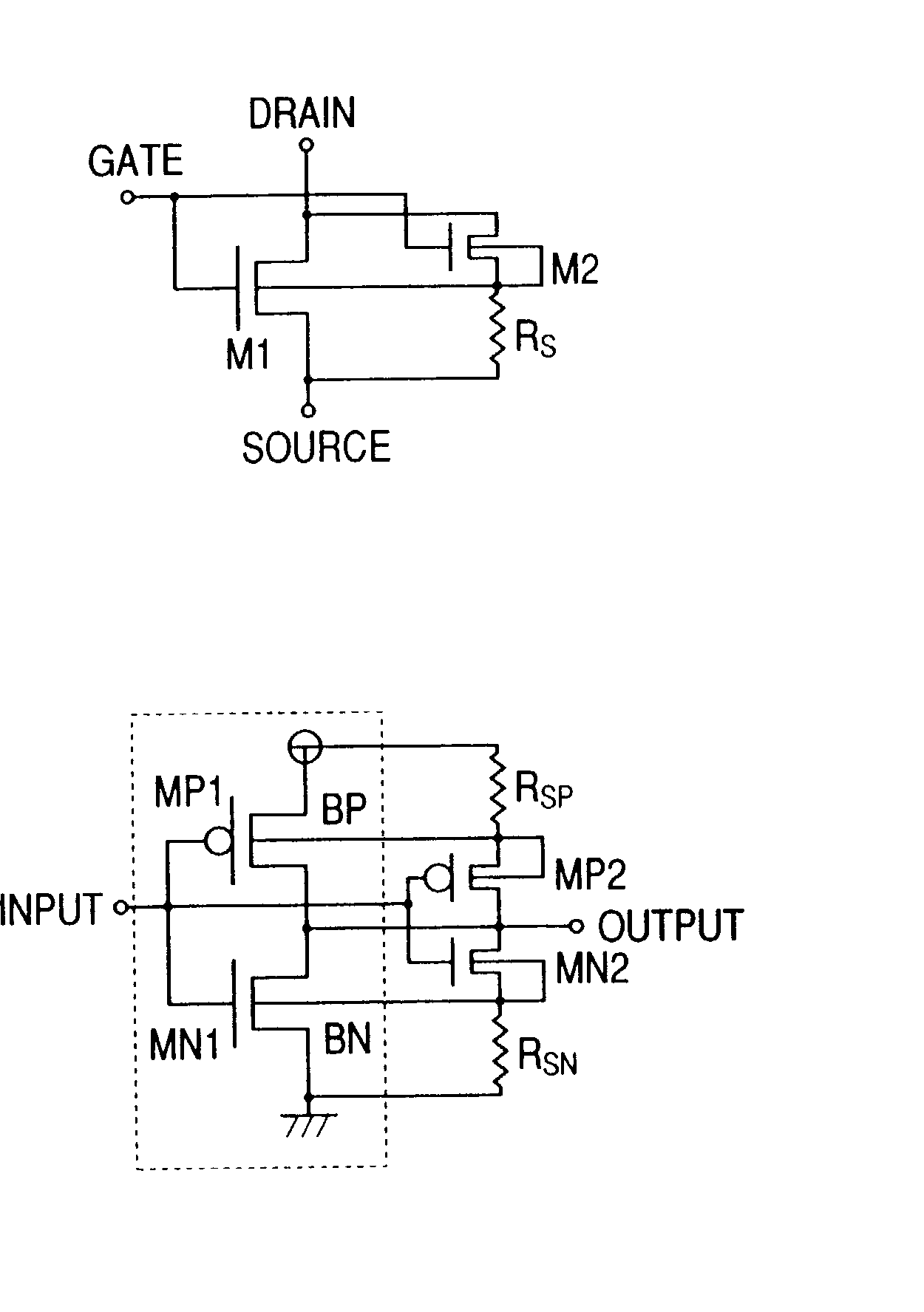
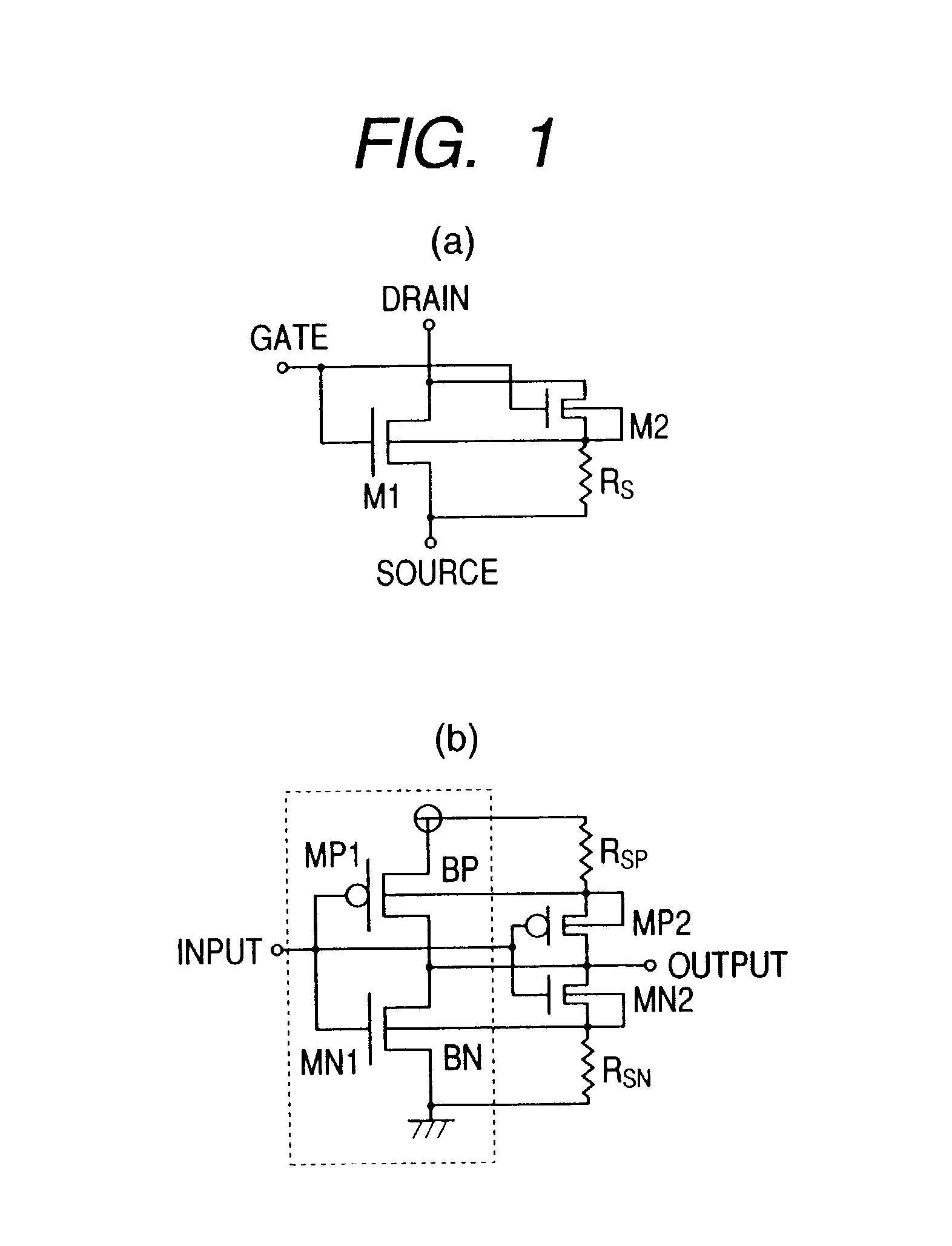
[0151] FIG. 8 is a plan view of a completed semiconductor integrated circuit according to a second embodiment of the present invention. FIG. 9 is a sectional view of the semiconductor integrated circuit, and FIG. 1(b) is a circuit configuration diagram of the semiconductor integrated circuit. FIGS. 10 and 11 show dynamic output properties and delay time properties, respectively, obtained by the semiconductor integrated circuit according to the second embodiment.

[0152] The second embodiment is an example of a semiconductor integrated circuit having a function as a CMOS inverter. A fundamental fabrication method of the second embodiment is the same as that of the first embodiment described above; however, process steps for forming CMOS are added to the fabrication method.

[0153] The fabrication process will now be described with reference to FIGS. 8 and 9. A modification only for formation of pMOS is made to the fabrication process, and a fundamental fabrication method...

Example

THIRD EMBODIMENT

[0166] FIG. 12(a) is a circuit configuration diagram of a semiconductor integrated circuit according to a third embodiment of the present invention. FIG. 13 is a plan view of the completed semiconductor integrated circuit, and FIG. 14 is a sectional view of the completed semiconductor integrated circuit. It should be noted that FIG. 13 shows only main parts, and reference numerals in the plan view of FIG. 13 denote parts as in the corresponding sectional view of FIG. 14.

[0167] The third embodiment is an example of a semiconductor integrated circuit without the transistor M2 of the first embodiment. This semiconductor integrated circuit has a capacitor instead of the transistor M2. More specifically, the semiconductor integrated circuit is provided with a capacitor having one electrode connected to a gate electrode of a first transistor and the other electrode connected a source of the first transistor via a body node of the first transistor and a first resistor.

[0168...


PUM


Abstract

A semiconductor integrated circuit according to the present invention comprises a MOS transistor formed on an SOI substrate and a subsidiary transistor provided between a body node and a drain node of the MOS transistor and sharing a gate electrode with the MOS transistor, whereby body potential of the MOS transistor is controlled by gate and drain potentials. Accumulated body charge in a non-conducting state in the semiconductor integrated circuit is extracted by a resistor formed between the body node and a source, whereby various phenomena caused by floating body effect are eliminated. Since the body potential of the MOS transistor can be varied without creating an undesirable leakage current path, and hence without limitations to supplied voltage, its threshold voltage can be made variable so as to follow change in an input signal, thereby making it possible to achieve higher speed and lower voltage operation of the semiconductor integrated circuit. According to the present invention, it is possible to eliminate floating body effect, which is the greatest problem with an SOI transistor formed on an SOI substrate, and also to achieve lower voltage and greater current operation of a transistor without posing limitations to supplied voltage and without causing the problem of leakage current.

Description

[0001] The present invention relates to a semiconductor integrated circuit. Semiconductor integrated circuits according to the present invention can be effectively applied to memories, electronic control units, and processor units that have such-semiconductor integrated circuits as components.[0002] A method of forming a MOS field effect transistor (hereinafter abbreviated to MOS) in a single crystalline semiconductor layer on an insulator is known as an SOI (Silicon On Insulator) MOS structure (hereinafter abbreviated to SOI.multidot.MOS) forming method. The MOS has a thick insulator directly thereunder, and therefore is characterized by its ability to reduce drain junction capacitance and signal line to substrate capacitance to about {fraction (1 / 10)} of those of conventional MOS. In addition, the MOS is insulated and separated from its supporting substrate, and therefore is also characterized by its ability to substantially eliminate drawback due to irradiation with .alpha. rays ...

Claims


Application Information

Patent Timeline
IPC IPC(8): H01L29/78H01L21/336H01L21/8234H01L21/84H01L27/088H01L27/12H01L29/76H01L29/786H01L29/94H01L31/062H01L31/072H01L31/113H01L31/119
CPCH01L27/1203H01L21/84
Inventor HORIUCHI, MASATADA
Owner HITACHI LTD
Why Eureka
Try Eureka