
Laser diode

a laser diode and diode technology, applied in the field of laser diodes, can solve the problems of weak reflection return light, difficult to achieve high light-emission efficiency, and deterioration of single wavelength characteristi

Inactive Publication Date: 2003-05-22
FUJITSU LTD
View PDF4 Cites 4 Cited by
  • Summary
  • Abstract
  • Description
  • Claims
  • Application Information

AI Technical Summary

Benefits of technology

[0024] This arrangement can efficiently prevent refractive-index-coupling, while maintaining superiority in single-wavelength characteristics. In addition, the degree of freedom for design of the laser structure is large.

Problems solved by technology

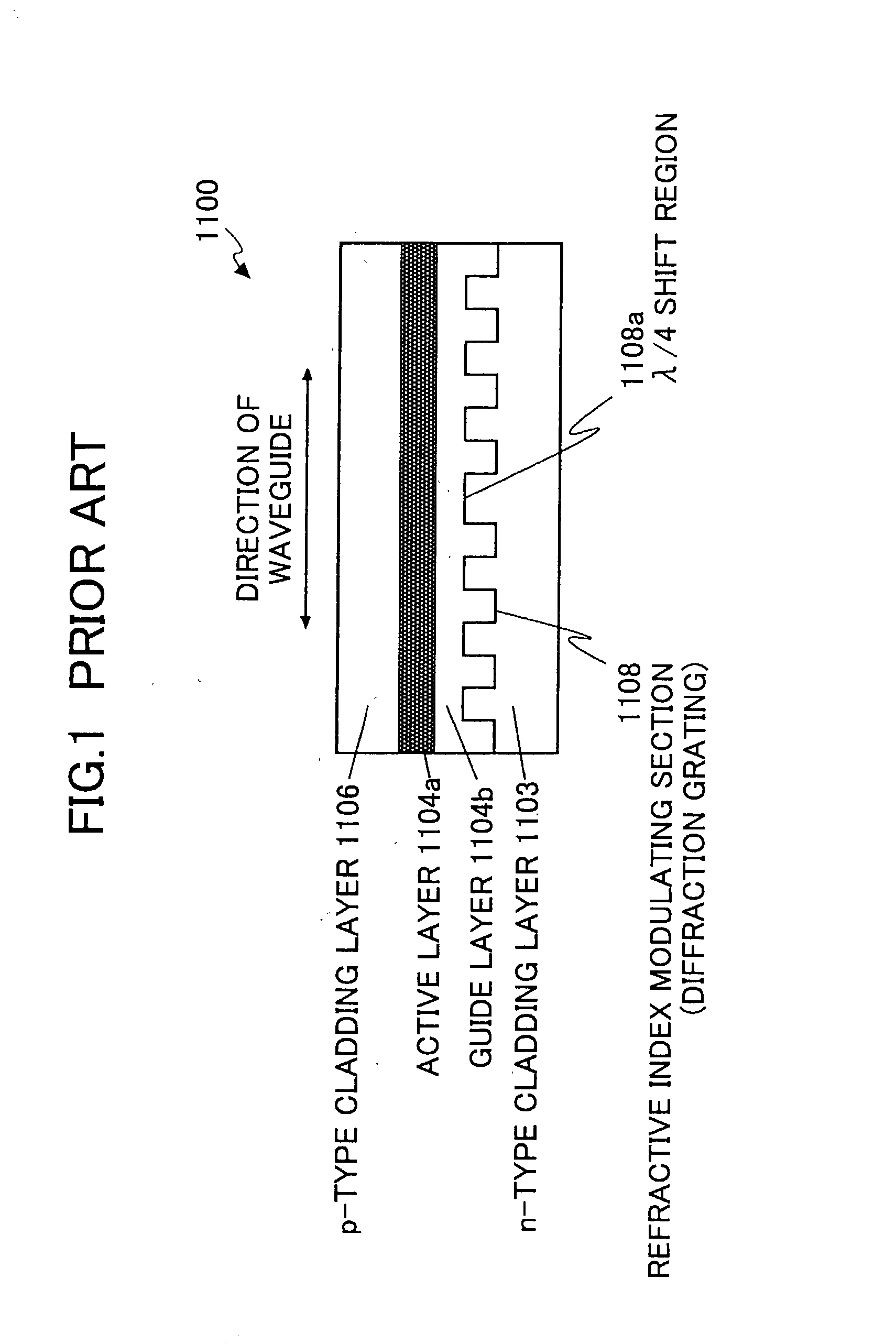
Another problem in the conventional .lambda. / 4 phase-shift refractive-index-coupled DFB laser 1100 is the difficulty of achieving a high light-emission efficiency because both ends of the resonator are covered with anti-reflective (AR) coating.
Furthermore, it is difficult for the conventional .lambda. / 4 phase-shift refractive-index-coupled DFB laser 1100 to increase the normalized coupling factor (.kappa.L), and therefore, it is weak for reflected return light.
However, if the internal light intensity increases, the electric field within the resonator increases, and spatial hole burning (SHB) is more likely to occur, causing deterioration of the characteristic of single wavelength.
However, the above-described advantages are limited to a pure gain-coupled DFB laser, in which gain modulation solely exists without other components.
As a realistic problem, it is very difficult to fabricate a pure gain-coupled DFB laser.
However, this technique requires strict and precise control of the thickness of each semiconductor film.
This requirement reduces the degree of freedom for design of the laser structure.
In addition, the degree of freedom for design of the laser structure is large.

Method used


Image

  • Laser diode
  • Laser diode
  • Laser diode

Examples


first embodiment

[0052] First Embodiment

[0053] FIGS. 4 through 6 illustrate a gain-coupled DFB laser 100 according to the first embodiment of the invention. In the first embodiment, the gain-coupled DFB laser 100 is fabricated on an indium phosphide (InP) substrate and oscillates at 1.3 .mu.m (microns) region.

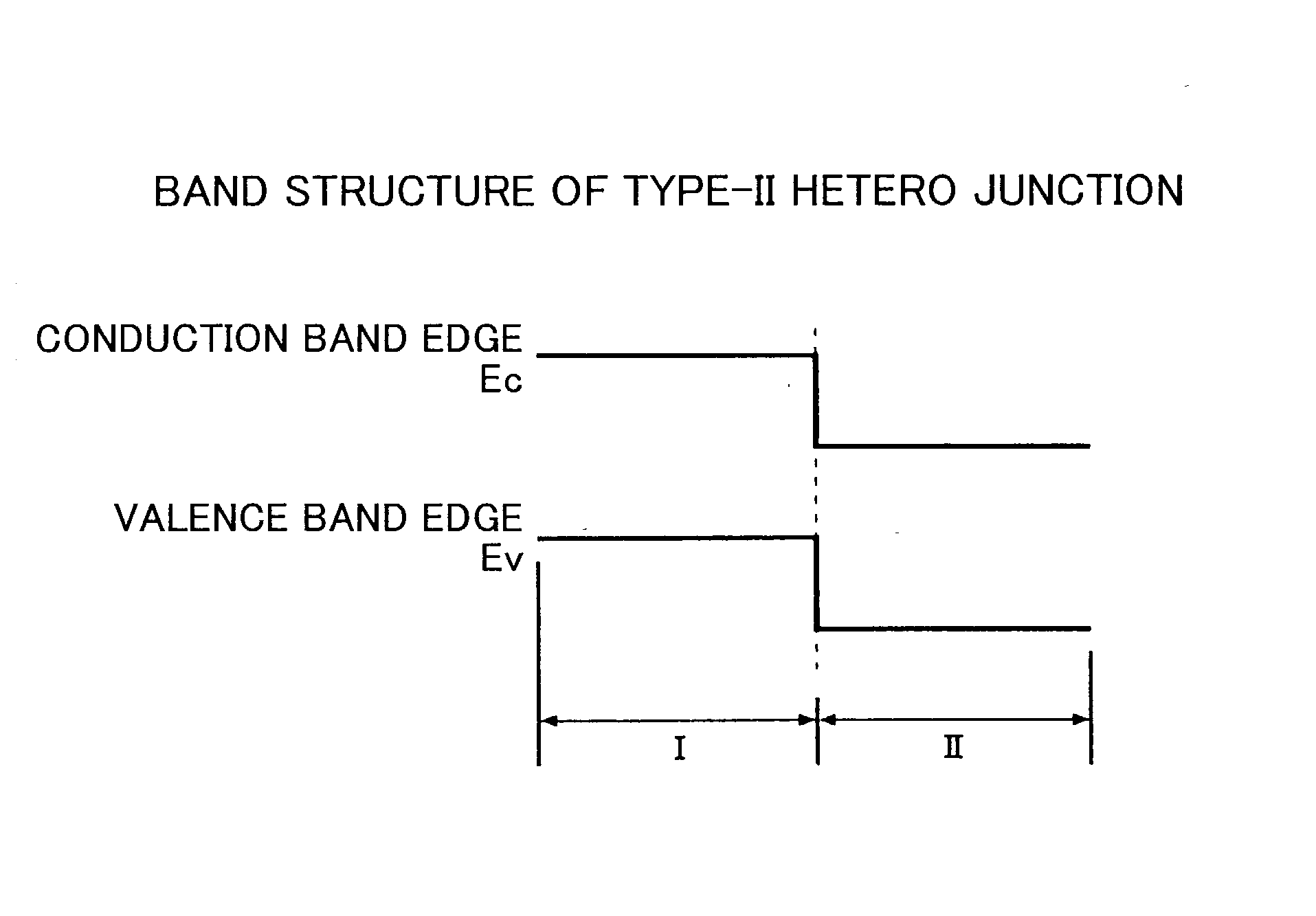
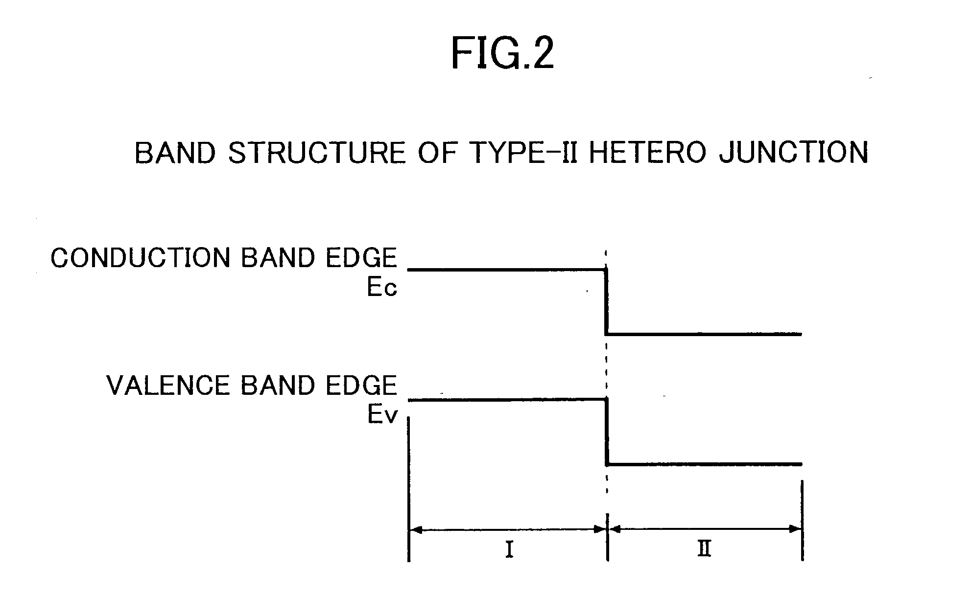
[0054] To define type-II hetero junction in the active layer, bulk crystal of antimony compound semiconductor material is used; however, any other materials that can define a type-II band structure can also be used.

[0055] FIG. 4A is a cross-sectional view of the gain-coupled DFB laser 100 taken along a plane perpendicular to the longitudinal axis of waveguide (i.e, the active layer), and FIG. 4B is a cross-sectional view of the active layer 104a of the gain-coupled DFB laser 100 taken along the longitudinal axis of the waveguide.

[0056] In FIG. 4A, the gain-coupled DFB laser 100 is fabricated on an n-type InP substrate 101 doped with n-type impurities. An n-type InP cladding layer 102 with a thi...

second embodiment

[0076] Second Embodiment

[0077] FIG. 7A and FIG. 7B illustrate a gain-coupled DFB laser 200 according to the second embodiment of the invention. Type-II hetero junction of bulk crystals of homogeneous semiconductors explained in the first embodiment is applicable to a SQW (strained quantum well) structure or a MQW (multiple quantum well) structure. Accordingly, in the second embodiment, a gain-coupled DFB laser diode 200 has an active layer with an MQW structure including an InGaAsP quantum well that has a lattice constant matched with the InP substrate.

[0078] FIG. 7A is a cross-sectional view of the gain-coupled DFB laser 200 taken along the longitudinal axis of waveguide, and FIG. 7B is an enlarged view of the MQW structure having type-II hetero junction. The same elements as those shown in the first embodiment are denoted by the same numerical references, and explanation for them will be omitted.

[0079] The gain-coupled DFB laser 200 has a core 204 that includes an active layer 204...


PUM


Abstract

A laser diode comprises a first cladding layer having a first conductivity, a second cladding layer having a second conductivity, an active layer located between the first cladding layer and the second cladding layer and extending from one end surface to the other end surface, a first electrode configured to inject a carrier with a first polarity into the active layer via the first cladding layer, and a second electrode configured to inject a carrier with a second polarity into the active layer via the second cladding layer. The active layer comprises a first active region and a second active region, which are arranged alternately and periodically from one end surface to the other end surface in the direction of light propagation, and the first active region and the second active region define type-II hetero junction between them.

Description

[0001] 1. Field of the Invention[0002] The present invention generally relates to a laser diode, and more particularly to a gain-coupled distributed-feedback laser diode.[0003] 2. Description of the Related Art[0004] Currently, wavelength division multiplexing (WDM) techniques are employed in the backbone transmission system of a high-capacity optical communication network. WDM is a technique for multiplexing optical signals on the wavelength axis to improve the transmission capacity.[0005] The ITU-T grid, which is one of the ITU-T Recommendations announced by the Telecommunication Standardization Sector of the International Telecommunication Union (ITU-T), strictly defines the wavelength and the wavelength interval used in WDM. For this reason, the oscillation wavelength of the laser used as a light source has to be precisely controlled so as to be in conformity with the TTU-T grid.[0006] A refractive index modulated distribution-feedback laser having a quarter wave (.lambda. / 4) ph...

Claims


Application Information

Patent Timeline
IPC IPC(8): H01S5/12H01S5/32H01S5/323H01S5/34H01S5/343
CPCB82Y20/00H01S5/3422H01S5/322H01S5/1228
Inventor SEKINE, NORIHIKO
Owner FUJITSU LTD
Learn More