

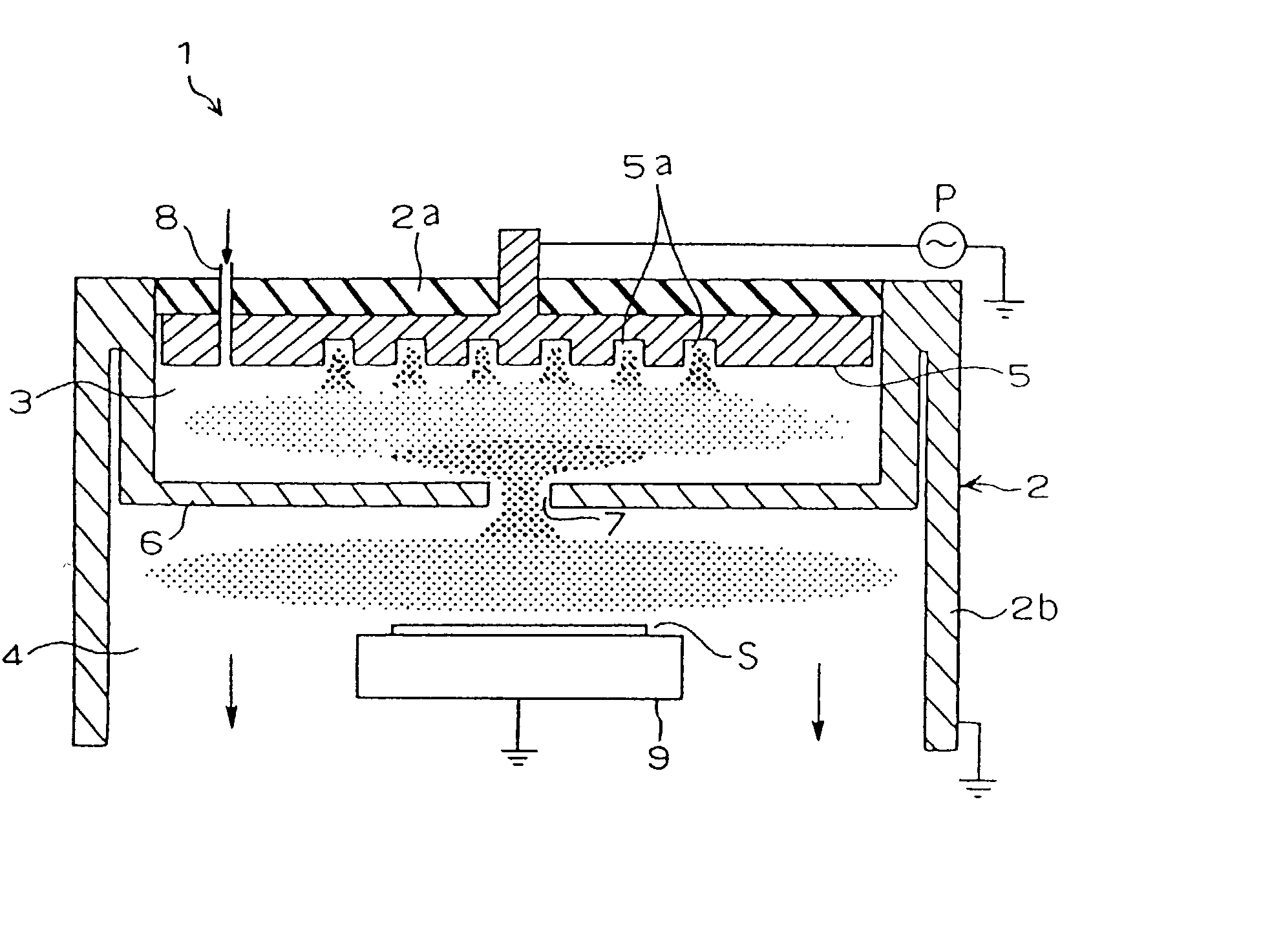
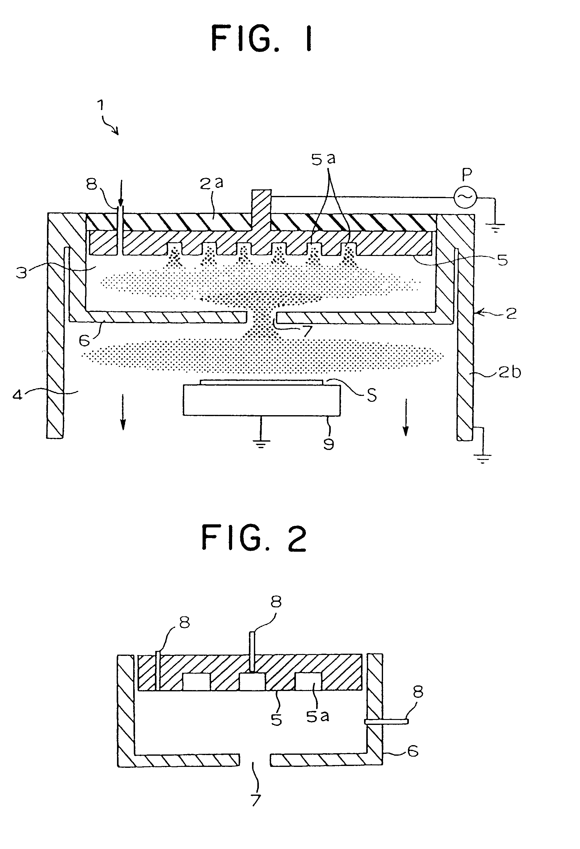
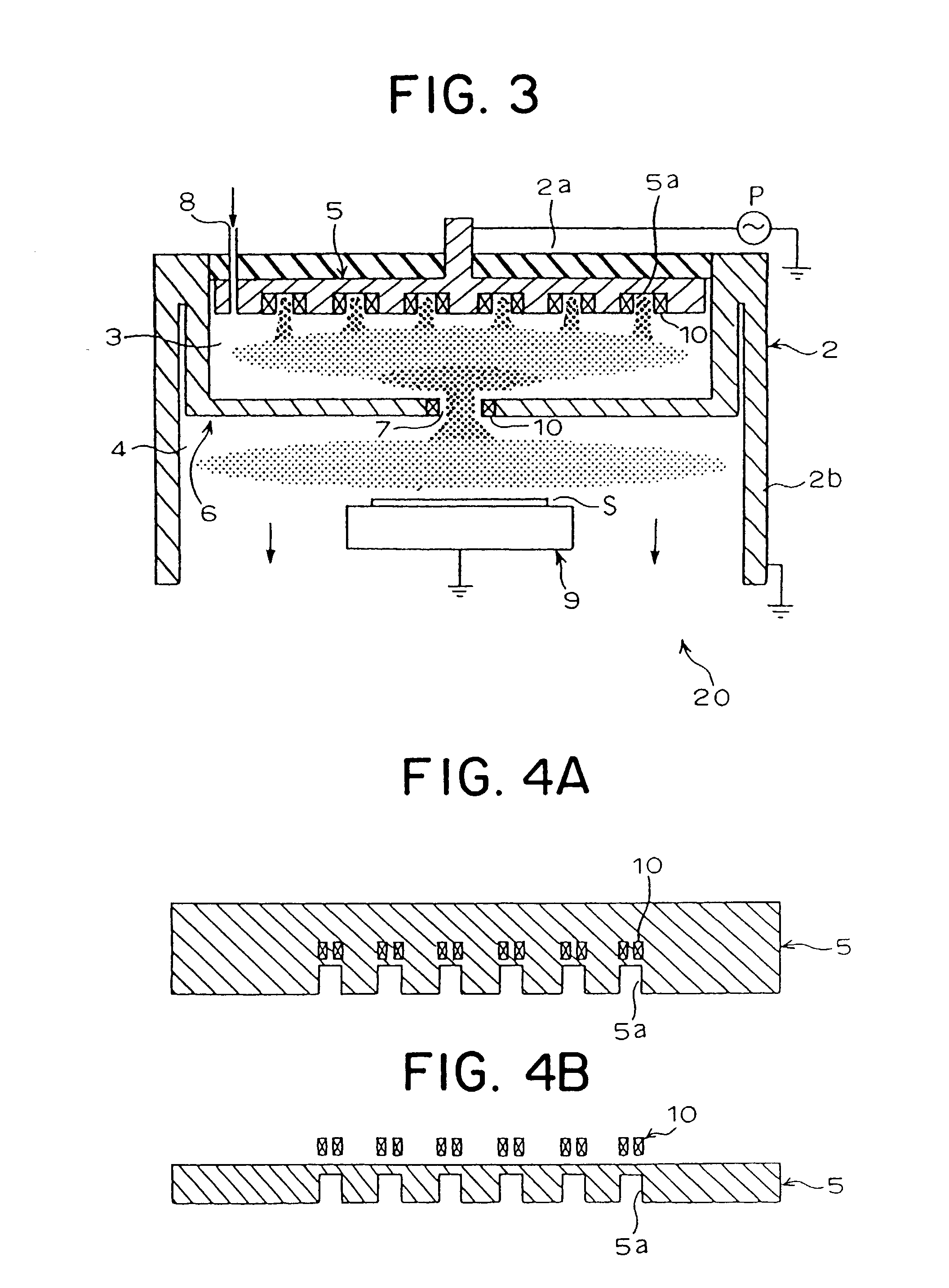
Surface treatment apparatus
a surface treatment and apparatus technology, applied in the direction of coatings, chemical vapor deposition coatings, electric discharge tubes, etc., can solve the problems of low throughput, high cost, and deterioration of the film quality of the substra
- Summary
- Abstract
- Description
- Claims
- Application Information
AI Technical Summary
Benefits of technology
Problems solved by technology
Method used
Image

Examples
example 2
[0290] The plasma nozzle 57 shown in FIG. 43 is adopted for silicone thin film formation treatment as in Example 1, be setting the slit width W1 in the vicinity of the center of the partition plate to 8.0 mm, the slit width W2 in the vicinity of the outer circumference to 6.0 mm, and the whorl interval D to 8.0 mm. As a result, crystalline silicone thin film was obtained, and its film thickness distribution was more uniformed than Example 1.
3 TABLE 3 Example 1 Example 2 Plasma nozzle shape Whorl slit shape Whorl slit shape Slit width W: Constant Slit width W: Variable 8.0 mm W1 8.0 mm Whorl interval L: W2 6.0 mm 8.0 mm Whorl interval L: 8.0 mm Anode electrode 7.0 mm 7.0 mm thickness Film thickness 0.75 1.00 distribution (uniformity)* Film nature Crystalline Crystalline *The film thickness distribution is normalized by dividing the thinnest portion of the formed film by the thickest portion.
[0291] A plasma nozzle 58 shown in FIGS. 44A and 44B has a whorl shaped top surface and a cons...
PUM
| Property | Measurement | Unit |
|---|---|---|
| Temperature | aaaaa | aaaaa |
| Length | aaaaa | aaaaa |
| Length | aaaaa | aaaaa |
Abstract
Description
Claims
Application Information