
Optoelectric module for multi-fiber arrays

a multi-fiber array, optoelectric module technology, applied in the field of small form factor optoelectric modules, can solve the problems of small form factor designs, increased space required, and prone to limi

Inactive Publication Date: 2003-07-24
TE CONNECTIVITY CORP
View PDF18 Cites 65 Cited by
  • Summary
  • Abstract
  • Description
  • Claims
  • Application Information

AI Technical Summary

Benefits of technology

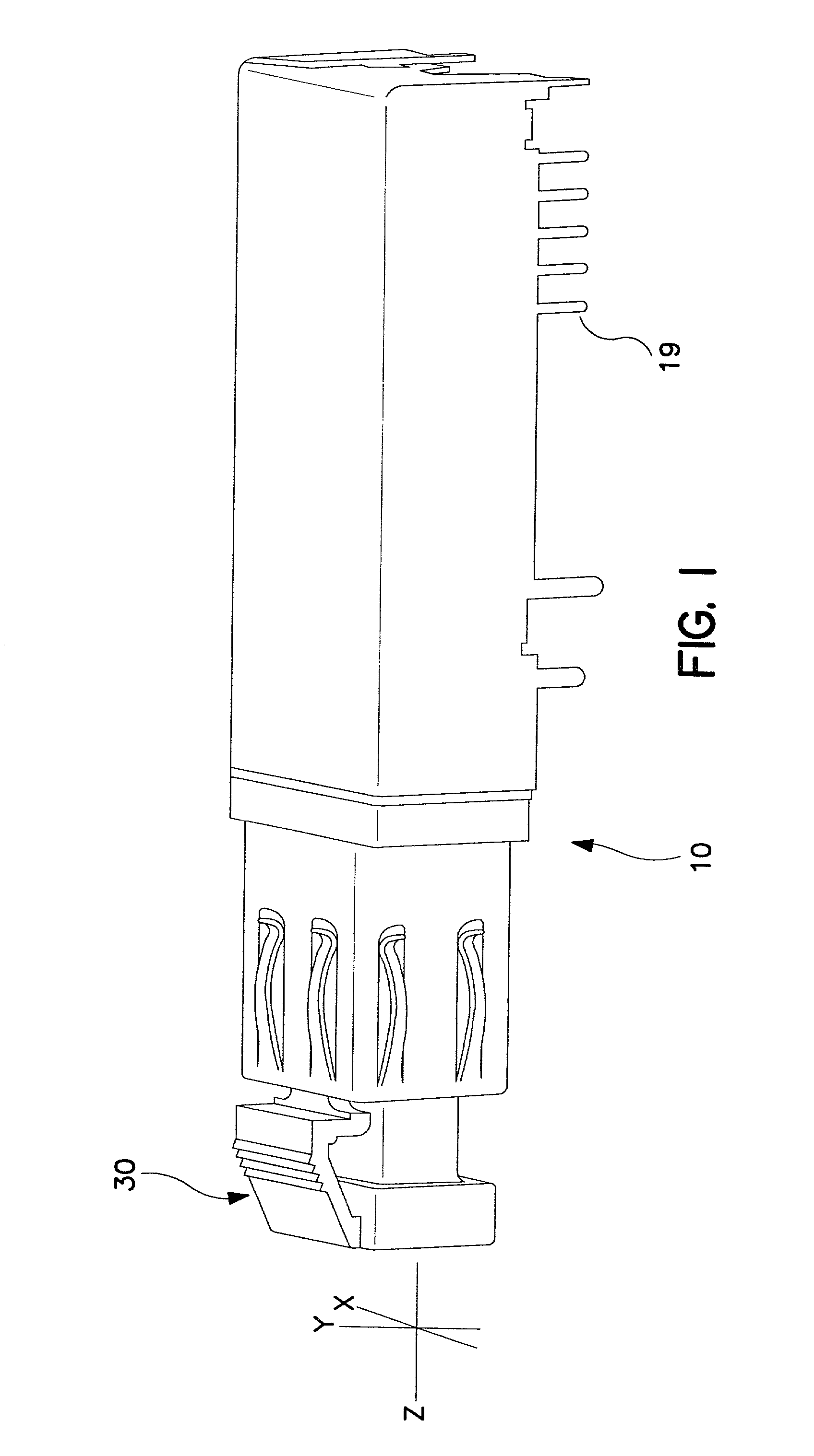
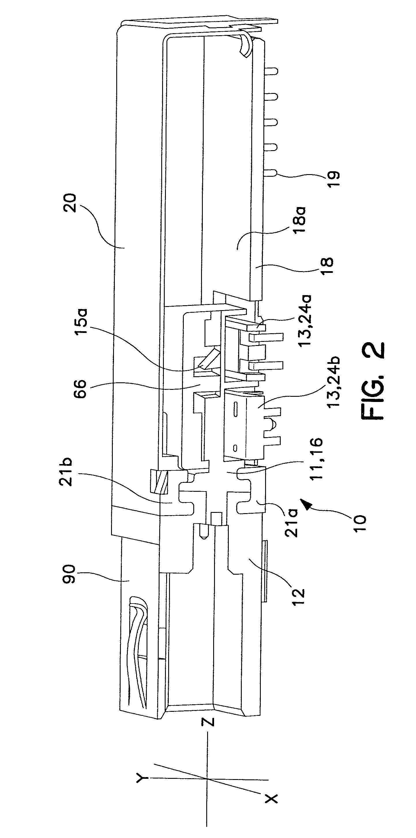
[0014] Significant advantages have been realized by separating the OEDs along the y,z axes while maintaining their alignment along the x-axis. First, as mentioned above, such a configuration may increase space between the OEDs, and, at the very least, avoids having to optically communicate with the OEDs within the same area as the x,y array of the fiber assembly. Additionally, the configuration does not increase the space required along the x-axis, which, in small form factors designs, tends to limit due to the fact that the fibers typically extend in rows along the x-axis in the multi-fiber array. The configuration of the present invention is particularly advantageous when the OEDs are staggered along the z axis since modules tend to have more flexibility with respect along the z-axis then either the x or y-axes. In other words, since the module is typically elongated along the z-axis, maximum separation can be achieved between OEDs along this axes. Furthermore, by increasing separation, cross talk between the OEDs can be minimized.
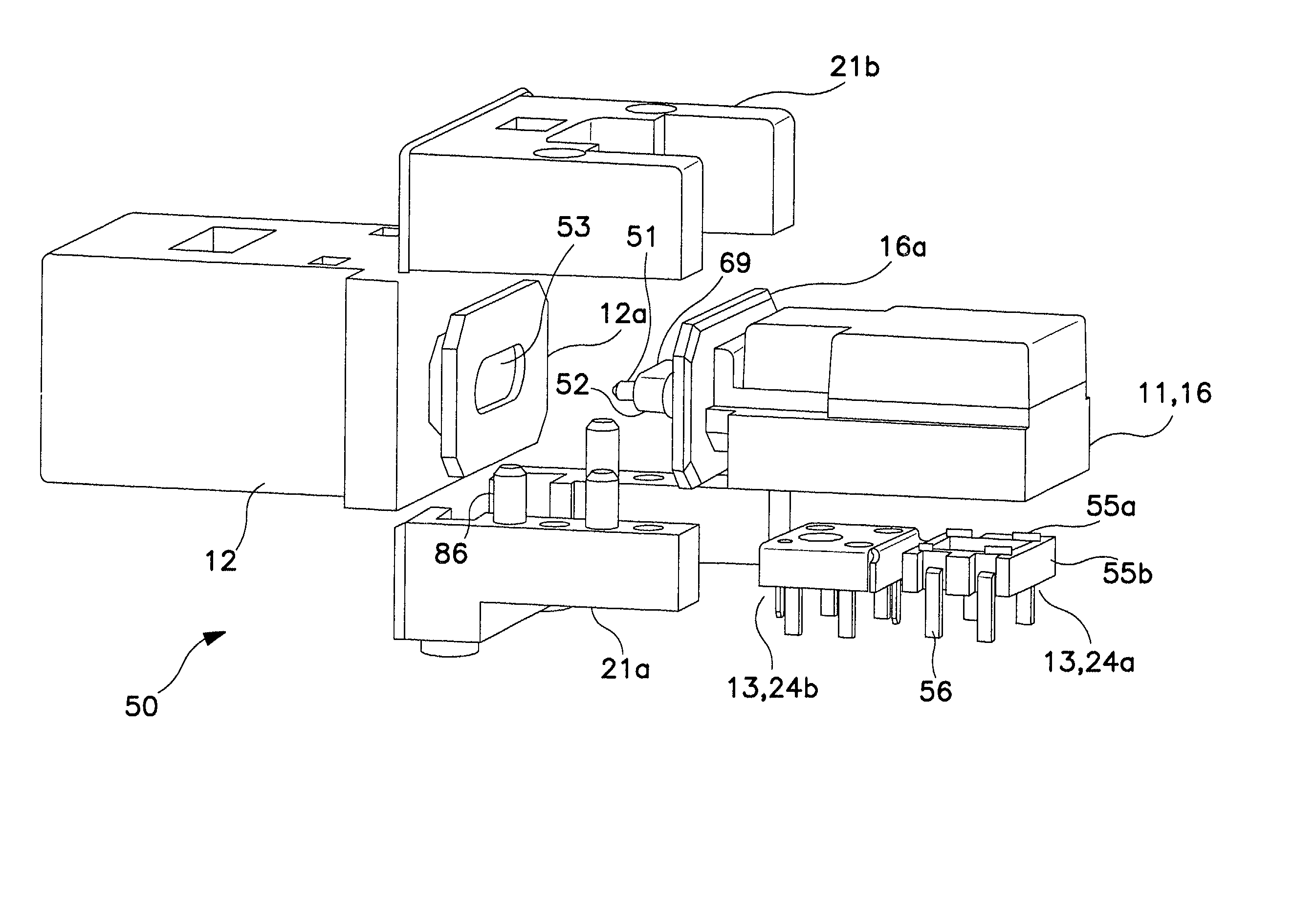
[0017] The optical block of the present invention can be used to form an optical subassembly in which all critical optical alignments are contained. To this end, aside from defining optical paths, the optical block preferably comprises alignment features on one end to align the optical block with an optical connector, and receptacles on the other end to receive and align the OEDs. Such an optical subassembly therefore can be handled as a component part which eases assembly of the module not only by eliminating optical alignment steps, but also by providing a robust component suitable for automated handling.
[0020] The feedback approach of the present invention offers several key advantages. For example, since a portion of the entire beam is reflected back to the monitor, average power can be measured precisely and there is no need to approximate as in prior art devices. Furthermore, in a preferred embodiment, the light is reflected along the same plane as the transmitted light and therefore is able to use the same reflective surface that the transmitted light uses to change direction. Additionally, since the reflected light is being directed to a photo diode, which typically has a relatively large surface area, there is generally a great deal of tolerance in the placement of the partially-reflective surface. And finally, the optical block of the present invention can be modified to accommodate the feedback system of the present invention with very little effort and expense. Specifically, all that is needed is a cavity angled at a certain degree to avoid reflecting the light along the same axis as the transmitted light. The mirror or partially-reflective surface that is inserted into the cavity is inexpensive flat glass coated in conventional ways. Therefore, in addition to accommodating the light bending in the parallel optics of the present invention, the feedback approach of the present invention also offers higher quality, greatest simplicity and lower cost then comparable feedback systems used in traditional TO cans.
[0024] Still another aspect of the present invention is an assembly method which avoids distorting critical optical alignments during assembly. In a preferred embodiment, the method comprises: (a) providing an optical assembly containing substantially all of the optical alignments from a cable assembly interface to at least one OED including the optical alignment of the OED; (b) assembling the module at least to the extend that a circuit board to which the OED is to be connected is held rigidly in relation to the optical assembly; and (c) after step (b), electrically connecting the OED to the circuit board.

Problems solved by technology

Additionally, the configuration does not increase the space required along the x-axis, which, in small form factors designs, tends to limit due to the fact that the fibers typically extend in rows along the x-axis in the multi-fiber array.

Method used


Image

  • Optoelectric module for multi-fiber arrays
  • Optoelectric module for multi-fiber arrays
  • Optoelectric module for multi-fiber arrays

Examples


example

[0071] The optical block 16 of FIG. 6 and the optical paths it defines, including its feedback configuration, are described in particular detailed with respect to the ray tracing diagrams shown in FIGS. 7(a)-(c). It should be understood that optical block 16 and the optical paths defined therein are merely represented of the invention, and not exhaustive. For example, optical block 16 is used in a transceiver and defines two optical paths: one path couples optical signals from a fiber to a photodetector, while the other path couples optical signals from the OED to the fiber. Clearly, however, the present invention covers more than just two optical paths, and the optical paths can be used for propagating signals in either direction.

[0072] FIG. 7(a) shows the design concept of the transmitter. The light from a VCSEL on a lead frame 24a goes through a second lens 67a on its way to the coupled fiber. To accommodate the oxide VCSEL's large divergent angle, the optical lens 67a has a 1.4:...


PUM


Abstract

An optoelectric module adapted to cooperate with a multi-fiber array by displacing a plurality of OEDs from the fiber array at least along the z,y-axes or a combination thereof while maintaining their alignment along either the x-axis of the fiber array, the module comprising: (a) a connector interface adapted to interconnect with a multi-fiber assembly having an x,y array of fibers; (b) a plurality of OEDs for converting between optical and electrical signals; and (c) optical paths wherein each optical path has a first end adapted for optically coupling with a corresponding fiber in an x,y array of fibers and a second end for optically coupling with a corresponding OED, wherein the distance between the second ends of at least two optical paths is greater than the distance between their corresponding first ends and wherein the distance across the second ends along the x-axis is no greater than the distance across the first ends along the x-axis.

Description

[0001] The present invention is related generally to optoelectric devices. More specifically, the present invention relates to optoelectric devices for use with multi-fiber arrays.[0002] As technology continues to evolve in telecommunications, optics is playing an ever-increasing role and, in many respects, has become predominant over conventional electrical transmissions. An important subsystem of an optical telecommunication system is the optoelectric interface which converts signals between the optical domain and the electrical domain. Typically, the optoelectric interface comprises some kind of optoelectric device (OED) for either transmitting or receiving optical signals. OEDs are commonly packaged in "TO can" assemblies which comprise a cap and a header assembly. The header assembly can be a hybrid microelectronic assembly which includes the OED plus one or more integrated circuits (ICs) or passive components. The header assembly includes an insulating plate, such as a suitabl...

Claims


Application Information

Patent Timeline
IPC IPC(8): G02B6/42
CPCG02B6/4214G02B6/4292G02B6/4249G02B6/4244G02B6/4261G02B6/4277G02B6/428G02B6/4286
Inventor O'TOOLE, MICHAEL M.LEVIN, BRADLEY S.EDWARDS, PHILLIP J.XU, LEE L.VANDENBERG, JOSEPH J.MARKHAM, JOSEPH
Owner TE CONNECTIVITY CORP
Learn More