Element transfer method, element arrangmenet method using the same, and image display

a transfer method and element technology, applied in the manufacture of electrode systems, electric discharge tubes/lamps, instruments, etc., can solve the problems of difficult to heat only the desired parts, positional deviation and peeling of other parts, and complicated work, so as to improve the fabrication yield of the image display unit, reduce the number of transfer, and reduce the effect of the number of transfer

Inactive Publication Date: 2003-08-28
XIAMEN SANAN OPTOELECTRONICS CO LTD
View PDF13 Cites 75 Cited by
  • Summary
  • Abstract
  • Description
  • Claims
  • Application Information

AI Technical Summary

Benefits of technology

0138] In the two-step enlarged transfer shown in FIGS. 6(a) to 6(d), each device 11 is covered with the resin and electrode pads are formed on the resin portion covering the device 11 by making use of the enlarged distance between adjacent two of the devices 12 after the first transfer, and wiring can be performed after the second transfer without occurrence of any connection failure by making use of the previously formed electrode pads and the like. As a result, it is possible to improve a fabrication yield of the image display unit.
0139] The two-step enlarged transfer method according to this embodiment includes the two enlarged transfer steps in each of which the devices are enlargedly spaced from each other. By performing a plurality of such enlarged transfer steps in each of which the devices are enlargedly spaced from each other, the number of transfer can be actually reduced. For example, assuming that an enlargement ratio between the pitch of the devices 12 on the temporarily holding member 11 (11a) and the pitch of the devices 12 on the first substrate 10 (10a) is taken as 2 (n=2) and an enlargement ratio between the pitch of the devices 12 on the second substrate 15 and the pitch of the devices 12 on the temporarily holding member 11 (11a) is taken as 2 (m=2), the total enlargement ratio becomes 2.times.2=4. To realize the total enlargement ratio (=4), according to a one-step transfer method, the number of transfer (alignment) of the devices 12 from the first substrate 10 to the second substrate 15 becomes 16. (=4.sup.2) On the contrary, to realize the same total enlargement ratio (=4), according to the two-step enlarged transfer method of this embodiment, the number of transfer (alignment) is obtained by simply adding a square of the enlargement ratio (=2) in the first transferring step to a square of the enlargement ratio (=2) in the second transferring step, with a result that the number of transfer becomes 8 (=4+4). Specifically, according to the two-step enlarged transfer method, to achieve the total enlargement ratio (transfer magnification) of n.times.m, the total number of transfer becomes (n.sup.2+m.sup.2) times, while according to the one-step transfer method, to achieve the same total enlargement ratio (transfer magnification) of n.times.m, the number of transfer becomes (n+m).sup.2=n.sup.2+2 nm+m.sup.2. As a result, according to the two-step enlarged transfer method, the number of transfer can be made smaller than that according to the one-step transfer method by 2 nm times, thereby correspondingly saving time and cost required for the fabrication step. This becomes more useful as the total enlargement ratio becomes large.

Problems solved by technology

In particular, for an image display unit such as an LCD or PDP, device isolation cannot be performed, so that in general, at the beginning of the fabrication process, devices are formed in such a manner as to be spaced from each other with a pitch equivalent to a pixel pitch of the image display unit.
In the case of using such a method, however, there arises a problem that since the electronic parts must be placed one by one, the work becomes complicated, and since the entire substrate is heated, there occurs the positional deviation and peeling of other parts.
Parts to be transferred and parts not to be transferred can be selectively transferred by using the above transfer method; however, according to the existing technique, it is difficult to heat only the desired parts, and therefore, this method has been not put into practical use.
Accordingly, in general, it is required to coat portions, at which parts are to be placed, of the substrate with a resin, and therefore, it fails to solve the above-described problem associated with the complicated work.
Similarly, there may be considered a method of picking up electronic parts once from a supply source by using an attracting head and placing them on a substrate; however, in this method, if the entire substrate is heated in the case of fixedly transferring the electronic parts from the attracting head to the substrate, there may occur an inconvenience that other parts having been already fixed to the substrate be peeled therefrom.
In the case of performing overall heating by laser irradiation, if either of a thermoplastic resin and each part has a low light absorptivity against laser beams, there occurs a problem that the thermoplastic resin is not heated to a desired temperature.
This method, however, has problems that since a plurality of steps of picking up each device by the attracting head, moving the attracting head, and placing the device to the substrate are required to transfer the devices, the transfer process becomes complicated, and since a plurality of kinds of equipment are required to be provided, the cost is raised, and that since the devices must be picked up one by one for mounting the devices, the mounting work becomes very complicated, and it takes much time to transfer the devices.
If it is intended to improve the working efficiency of the mounting machine for shortening the time required to mount the devices, there occurs another problem that the accuracy of arraying of the device at the time of mounting the devices is degraded.
Additionally, in the case of using the existing mounting machine, the positioning accuracy at the time of arraying devices has a limitation to about 10 .mu.m, and therefore, it is difficult to further enhance the positioning accuracy by the existing positioning method.

Method used


Image

  • Element transfer method, element arrangmenet method using the same, and image display
  • Element transfer method, element arrangmenet method using the same, and image display
  • Element transfer method, element arrangmenet method using the same, and image display

Examples


second embodiment

[0175] [Second Embodiment]

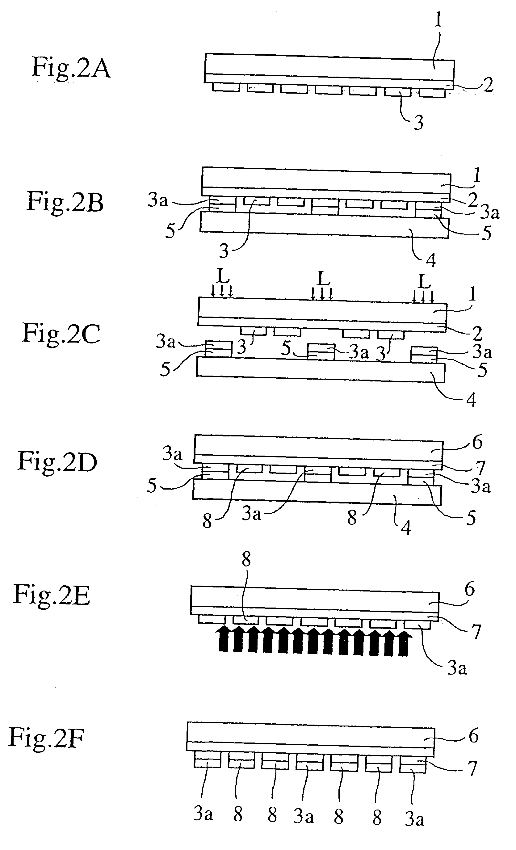
[0176] The second embodiment, which carries out each of the device transferring method, the device arraying method, and the image display unit fabricating method according to the present invention, will be described below. In this embodiment, parts corresponding to those described in the first embodiment are denoted by the same reference numerals and therefore the detailed description thereof is omitted.

[0177] [Device Transferring Method According to Second Embodiment]

[0178] The second embodiment is characterized in that an adhesive layer equivalent to the adhesive layer 7 according to the first embodiment contains a light absorbing material for increasing a light absorptivity of the adhesive layer against laser beams.

[0179] The light absorbing material for increasing a light absorptivity of the adhesive layer may be disposed in the vicinity of the adhesive layer. As such a light absorbing material contained in the adhesive layer or disposed in the vicinity...

third embodiment

[0201] [Third Embodiment]

[0202] The third embodiment, which carries out each of the device transferring method, the device arraying method, and the image display unit fabricating method according to the present invention, will be described below. In this embodiment, parts corresponding to those described in the first and second embodiments are denoted by the same reference numerals and therefore the detailed description thereof is omitted.

[0203] [Device Transferring Method According to Third Embodiment]

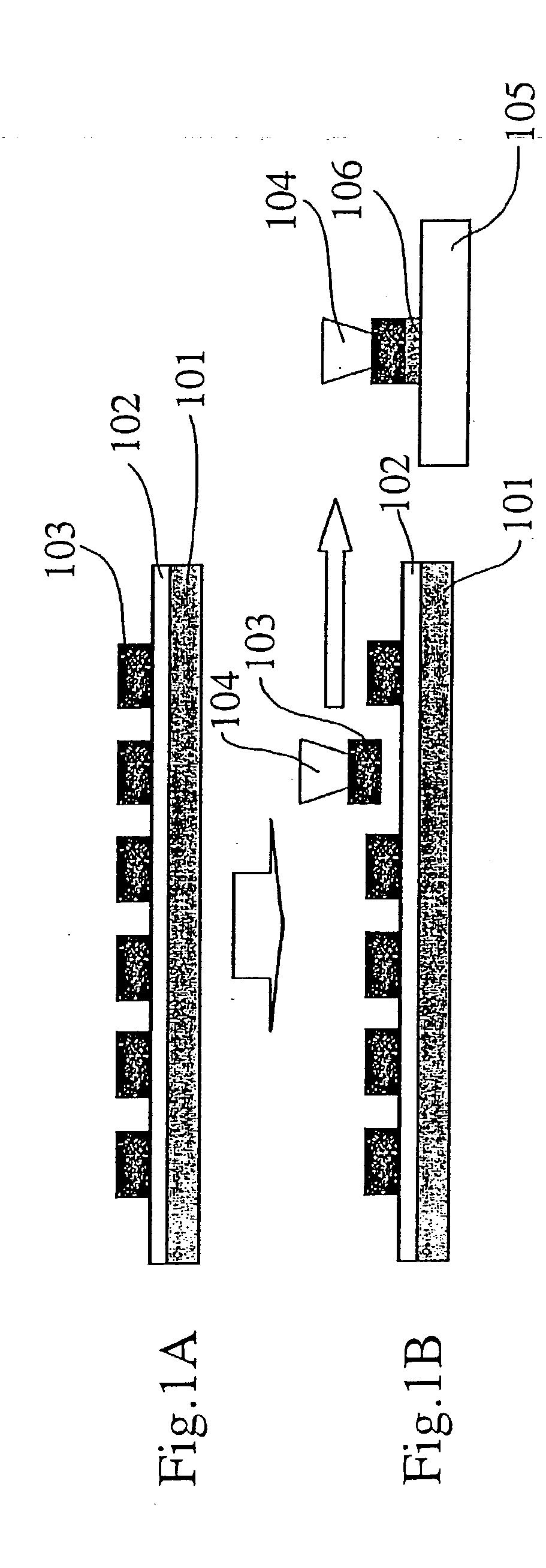
[0204] A device transferring method according to the third embodiment will be first described. To transfer devices 3 in accordance with the device transferring method of the present invention, as shown in FIG. 18(a), a thermal re-peelable layer 81 is formed on a base substrate 1 as a supply source, and a plurality of devices are formed in array on the base substrate 1.

[0205] The thermal re-peelable layer 81 has a property that the sticky force thereof is reduced when the layer 81 is h...


PUM

PropertyMeasurementUnit
sizeaaaaaaaaaa
sizeaaaaaaaaaa
thicknessaaaaaaaaaa

Abstract

A method of selectively transferring devices arrayed on a first substrate to a second substrate on which an adhesive resin layer is previously formed is disclosed. The method includes steps of selectively heating the adhesive resin layer on the second substrate by laser irradiation from the back surface side of the second substrate, and curing the selectively heated portions of the adhesive resin layer, thereby adhesively bonding those to be transferred of the devices to the second substrate. At this time, portions, corresponding to the devices, of the adhesive layer is heated directly or indirectly via the devices or wiring portions by laser irradiation from the back surface side of the substrate. The heated portions of the adhesive resin layer selectively exhibit the adhesive forces. The heated portions of the adhesive layer are then cured, so that only the devices to be transferred are selectively transferred to the second substrate. As a result, only the devices to be transferred can be certainly, efficiently, and accurately transferred without exerting adverse effect on other parts.

Description

[0001] The present invention relates to a device transferring method of transferring devices such as semiconductor light emitting devices, and a device arraying method and an image display unit fabricating method for transferring finely formed devices to a wider region by using the device transferring method.[0002] At present, an array of a number of fine devices, electronic parts, electronic devices, or electronic parts formed by burying the above devices or parts in an insulator such as a plastic material are being extensively used for electronic equipment.[0003] The assembly of an image display unit by arraying light emitting devices in a matrix is performed in two manners. For a liquid crystal display (LCD) or a plasma display panel (PDP), the light emitting devices are directly formed on a substrate, and for a light emitting diode display (LED display), single LED packages are arrayed on a substrate. In particular, for an image display unit such as an LCD or PDP, device isolati...

Claims


Application Information

Patent Timeline
Patent Type & Authority Applications(United States)
IPC IPC(8): B44C1/00B44C1/165H01L21/00H01L21/336H01L21/50H01L21/60H01L21/68H01L25/075
CPCH01L21/6835H01L2924/12041H01L24/82H01L25/0753H01L33/0079H01L33/20H01L2221/68318H01L2221/68354H01L2221/68359H01L2221/68368H01L2224/18H01L2224/82039H01L2924/01012H01L2924/01013H01L2924/01015H01L2924/0102H01L2924/01029H01L2924/01039H01L2924/01046H01L2924/01052H01L2924/01058H01L2924/01075H01L2924/01078H01L2924/01079H01L2924/3025H01L2924/01005H01L2924/01006H01L2924/01024H01L2924/01033H01L2924/014H01L24/18H01L21/568H01L24/24H01L2224/04105H01L2224/32225H01L2224/73267H01L2224/92244H01L2924/12042H01L33/0093H01L2924/00G02F1/136
Inventor HAYASHI, KUNIHIKOYANAGISAWA, YOSHIYUKIIWAFUCHI, TOSHIAKIOHBA, HISASHI
Owner XIAMEN SANAN OPTOELECTRONICS CO LTD
Why Eureka
Try Eureka