
Emitter turn-off thyristors and their drive circuits

a technology of turn-off thyristors and drive circuits, applied in the field of power electronics, can solve the problems of parasitic diodes, increased system size and complexity, poor safe operating area,

Inactive Publication Date: 2003-09-11
VIRGINIA TECH INTPROP INC
View PDF0 Cites 6 Cited by
  • Summary
  • Abstract
  • Description
  • Claims
  • Application Information

AI Technical Summary

Benefits of technology

[0013] A further purpose of this invention is to provide efficient drive circuits for the ETO thyristors. The drive circuit can block the turn-on command during the time when the anti-parallel diode conducting current. This function can save energy for the drive circuit and improve reliability of the ETO thyristor in a pulse width modulated (PWM) converter application condition.
[0014] Furthrmore, this invention provides a self-powered ETO dirve method. Using this method, no individual power input is needed for the driving circuit. This self-powered ETO thyristor and its drive circuit greatly improve the reliability and reduce the cost.
[0020] Another object of the present invention is to provide a novel ETO thyristor current sensing circuit and a new over-current detection circuit. The output of the current sensing circuit can be used for current control purpose and the output of the over-current detection circuit can be used for over-current protection purpose.

Problems solved by technology

Unfortunately, this latched state causes problems when the device turns off.
This is because some parts of the die (cells) remain latched even when the anode voltage begins to rise, leading to a poor safe operating area (SOA).
The discharge of this snubber capacitor requires significant power dissipation by a resistor or the use of complex energy recovery circuits, leading to increased system size and complexity.
However, when an anode short GTO thyristor or a transparent emitter GTO thyristor is used to build the ETO thyristor (this is the usual condition), there will be a parasitic diode present from gate to anode of the GTO thyristor.
If the ETO thyristor starts to block the positive voltage right after its parasitic diode conducting current, the ETO thyristor failure may occur due to the poor reverse recovery performance of the ETO thyristor's parasitic diode.
When the resonant current flow is into the gate and out of the cathode of the GTO thyristor, it may initiate a retriggering of the GTO thyristor, which leads to turn-off failure.
This mechanical structure makes the ETO thyristor difficult to produce.

Method used


Image

  • Emitter turn-off thyristors and their drive circuits
  • Emitter turn-off thyristors and their drive circuits
  • Emitter turn-off thyristors and their drive circuits

Examples


first embodiment

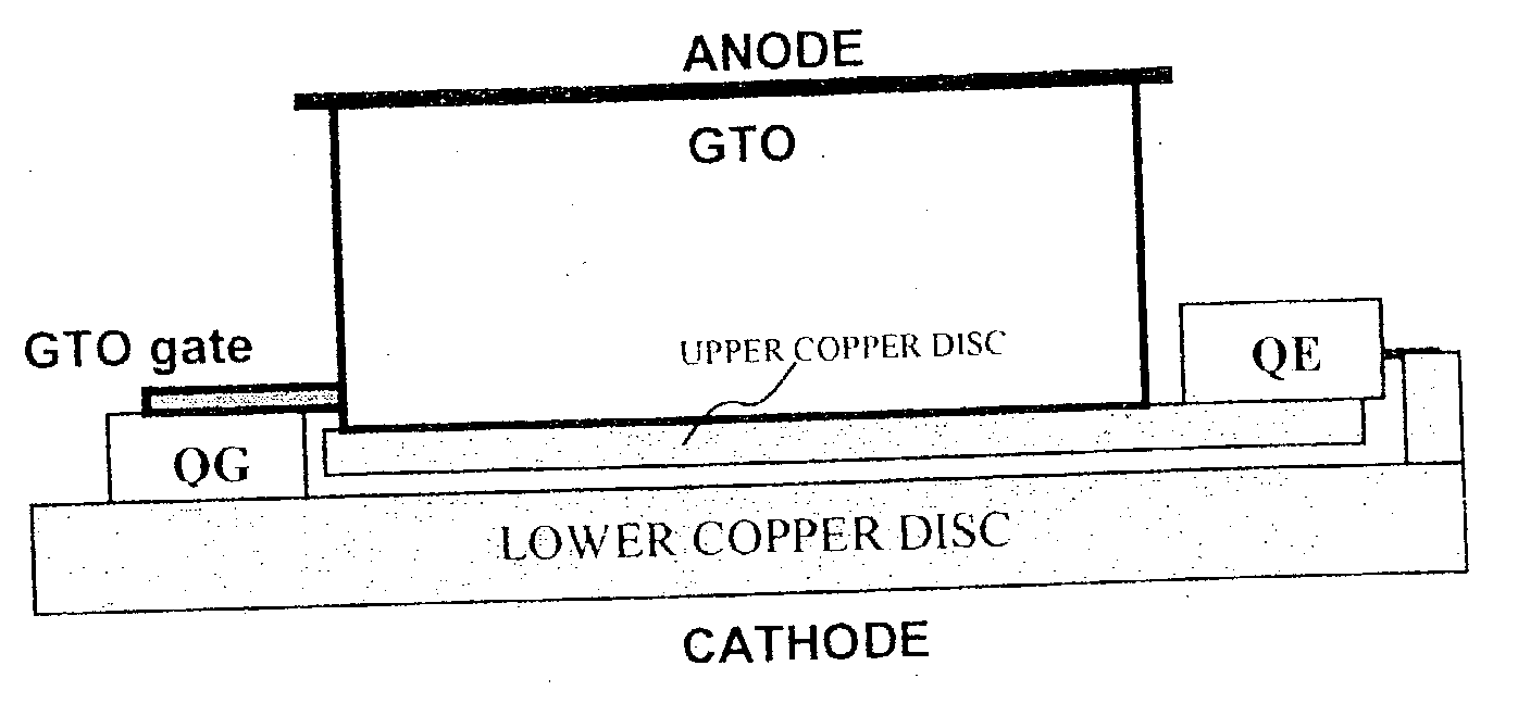
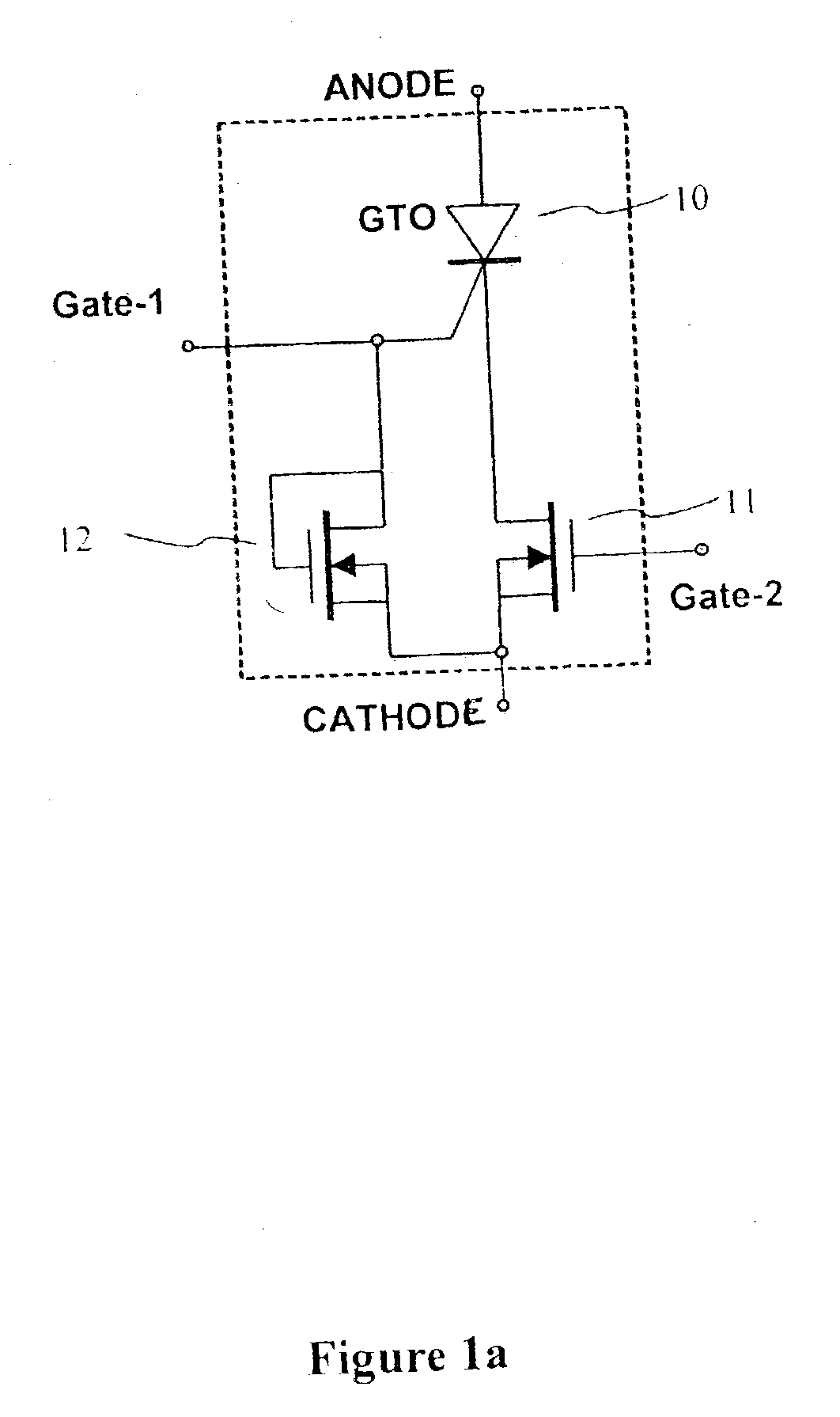
[0039] Referring again to the drawings, and more particularly now to FIG. 2, there is shown an equivalent circuit diagram of an ETO thyristor according to the invention. In this structure, a number (m pieces, in the depicted example, m=68) of paralleled MOSFETs, S.sub.11.about.S.sub.1m, are used to build the emitter switch. There are also resistors R.sub.11.about.R.sub.1m connect to the gates of the MOSFETs. The drains of S.sub.11.about.S.sub.1m connect to the cathode of the GTO thyristor. Between the cathodes of emitter switch S.sub.11.about.S.sub.1m and the gate of the GTO thyristor, there is a series circuit of a gate switch and a gate diode. A number (n pieces, in the depicted example, n=12) of paralleled MOSFETs, S.sub.11.about.S.sub.1n, are used to build the gate switch. There are resistors R.sub.11.about.R.sub.1n connect to the gates of the MOSFETs. And there are a number (i pieces, in the depicted example, i=12) of paralleled diodes, D.sub.11.about.D.sub.1i are used to build...

second embodiment

[0040] Referring now to FIG. 3 there is an equivalent circuit diagram of an ETO thyristor according to the invention. In this structure, a number (m pieces, in the depicted example, m=68) of paralleled MOSFETs, S.sub.11.about.S.sub.1m, are used to build the emitter switch. There are also resistors R.sub.11.about.R.sub.1m connect to the gates of the MOSFETs. The drains of S.sub.11.about.S.sub.1m connect to the cathode of the GTO thyristor. A number (n pieces, in the depicted example, n=12) of paralleled insulated gate bipolar transistors (IGBTs) S.sub.11.about.S.sub.1n, are used to build the gate switch. There are also resistors R.sub.11.about.R.sub.1n connect to the gates of the IGBTs. The anodes of S.sub.11.about.S.sub.1n connect the gate of GTO thyristor. The sources of S.sub.11.about.S.sub.1m and the sources of S.sub.11.about.S.sub.1n are connected together. The anode of the GTO thyristor, ANODE, and the sources of S.sub.11.about.S.sub.1n and S.sub.11.about.S.sub.1m, KATHODE1, ar...

third embodiment

[0041] Referring now to FIG. 4 there is an equivalent circuit diagram of an ETO thyristor according to the invention. In this structure, a number (mn pieces, in the depicted example, m=68) of paralleled MOSFETs, S.sub.11.about.S.sub.1m, are used to build the emitter switch. There are also resistors R.sub.11.about.R.sub.1m connect to the gates of the MOSFETs. The drains of S.sub.11.about.S.sub.1m connect to the cathode of the GTO thyristor. Between the cathodes of emitter switch S.sub.11.about.S.sub.1m and the gate of the GTO thyristor, there is a series circuit of a gate switch S.sub.2 and a capacitor C.sub.1. S.sub.2 has three terminals among which G is the control input. There is a diode D.sub.1 which is connected in parallel with C.sub.1. And there is a diode D.sub.2 which is connected in parallel with S.sub.2. The anode of the GTO thyristor ANODE, and the sources of S.sub.11.about.S.sub.1n KATHODE1 are defined the anode and the cathode of ETO thyristor respectively. There are fo...


PUM


Abstract

A family of emitter turn-off thyristors compres a gate turn-on (GTO) thyristor, a first switch, the drain of the first switch being connected to the cathode of the GTO thyristor, and a second switch connected between the gate of the GTO thyristor and the source of the first switch. The first switch consists of a number of paralleled metal oxide semiconductor field effect transistors (MOSFETs). The anode of the GTO thyristor and the source of the first switch serve as the annode and the cathode, respective, of the emitter turn-off thyristor. The emitter turn-off thyristor has four control electrodes; the gate of the GTO thyristor, the control electrode of the second switch, the gate of the first switch, and the cathode of the GTO thyristor.

Description

[0001] This application is related in subject matter to U.S. patent application Ser. No. 09 / 486,779 filed Mar. 2, 2000, by Alex Q. Huang for "Emitter Turn-off Thyristors (ETO)", the disclosure of which is incorporated herein by reference.DESCRIPTIONBackground of the Invention[0003] 1. Field of the Invention[0004] The present invention generally relates to the field of power electronics. More specifically, the present invention relates to several newly improved versions of the emitter turn-off thyristors and their drive circuits.[0005] 2. Background Description[0006] The gate turn-off (GTO) thyristor is a four-layer semiconductor device of the structure PNPN, usually fabricated on a single wafer up to six inches in diameter. In the on-state it exhibits a latching behavior which enables it to achieve very low conduction loss at a high current density. Unfortunately, this latched state causes problems when the device turns off. This is because some parts of the die (cells) remain latch...

Claims


Application Information

Patent Timeline
Patent Type & Authority Applications(United States)
IPC IPC(8): H01L23/60H01L27/02H01L29/417H01L29/744H03K17/567
CPCH01L23/60H01L27/0259H01L29/41716H01L29/744H01L2924/0002H03K17/567H01L2924/00
Inventor HUANG, OINZHANG, BIN
Owner VIRGINIA TECH INTPROP INC
Learn More