Method of plasma etching of high-K dielectric materials with high selectivity to underlying layers

a dielectric material and etching technology, applied in the field of dry etching of semiconductor wafers, can solve the problems of difficult to etch using conventional oxide etchants to form gate structures without damaging other, and the use of hafnium-oxide in semiconductor devices is limited, and the effect of improper operation or defective transistors

Inactive Publication Date: 2003-09-11
APPLIED MATERIALS INC
View PDF1 Cites 45 Cited by
  • Summary
  • Abstract
  • Description
  • Claims
  • Application Information

AI Technical Summary

Benefits of technology

0015] To facilitate understanding, identical reference numerals have been used,

Problems solved by technology

With such a thin dielectric, electrons can propagate from the polysilicon gate electrode into the transistor channel causing the transistor to operate improperly or become defective.
However, hafnium-oxide is such a stable dielectric mat

Method used


Image

  • Method of plasma etching of high-K dielectric materials with high selectivity to underlying layers
  • Method of plasma etching of high-K dielectric materials with high selectivity to underlying layers
  • Method of plasma etching of high-K dielectric materials with high selectivity to underlying layers

Examples


Embodiment Construction

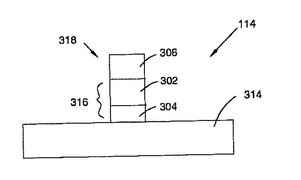
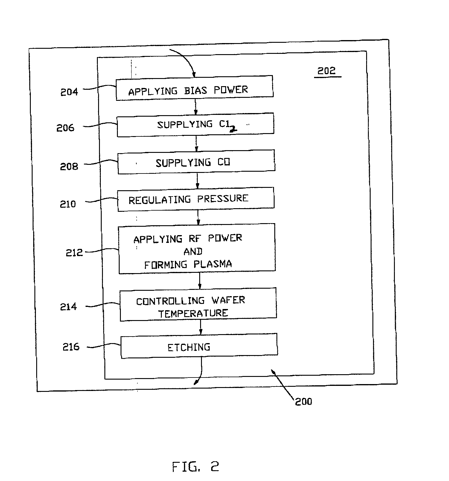
[0016] The present invention is a method of etching materials with high dielectric constants (high K materials have dielectric constants greater than 4.0) using a plasma generated from a gas (or gas mixture) comprising gases containing a halogen gas (such as Cl.sub.2, HCl and the like) and a reducing gas (such as carbon monoxide (CO). The high K materials include HfO.sub.2, ZrO.sub.2, Al.sub.2O.sub.3, BST, PZK, ZrSiO.sub.2, HfSiO.sub.2, TaO.sub.2, and the like. The type of halogen gas is selected to best remove the metal from the dielectric layer and the type of reducing gas is selected to best remove the oxygen from the dielectric layer. The etch process of the present invention can be reduced to practice in a Decoupled Plasma Source (DPS) Centura.RTM. etch system or a DPS-II etch system available from Applied Materials, Inc. of Santa Clara, Calif.

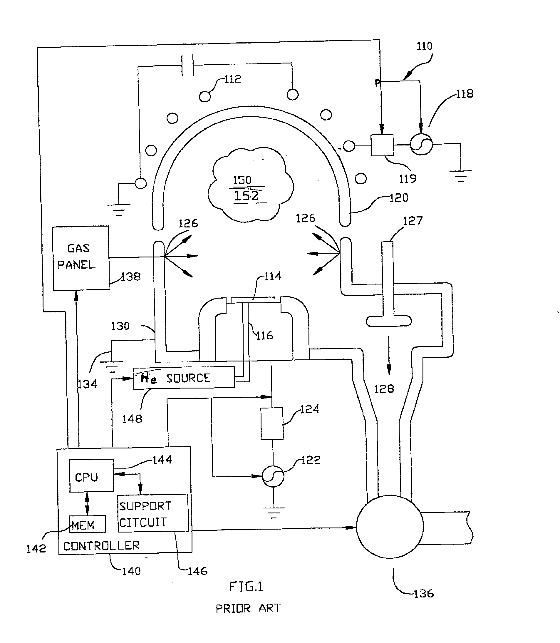
[0017] FIG. 1 depicts a schematic diagram of the DPS etch process chamber 110, that comprises at least one inductive coil antenna segmen...


PUM


Abstract

A method of etching high dielectric constant materials using halogen gas and reducing gas chemistry. An embodiment of the method is accomplished using a 20 to 300 sccm of chlorine and 2 to 200 sccm of carbon monoxide, regulated to a total chamber pressure of 2-100 mTorr to etch a hafnium oxide layer.

Description

[0001] 1. Field of Invention[0002] The present invention relates generally to a method of dry etching semiconductor wafers. More specifically, the invention relates to a method of etching high K dielectric materials using a gas mixture comprising a halogen gas and a reducing gas.[0003] 2. Description of the Background Art[0004] Field effect transistors that are used in forming integrated circuit generally utilize a polysilicon gate electrodes deposited upon a gate dielectric that separates the electrode from the channel between source and drain regions. In prior art transistor structures, the gate dielectric is typically fabricated of silicon dioxide (SiO.sub.2). However, as integrated circuit transistors have become smaller (on the order of 100 nanometers in width), the thickness of the dielectric material in the gate structure has become thinner than 10 Angstroms. With such a thin dielectric, electrons can propagate from the polysilicon gate electrode into the transistor channel c...

Claims


Application Information

Patent Timeline
IPC IPC(8): H01L21/311
CPCH01L21/31122H01L21/31116
Inventor NALLAN, PADMAPANI C.JIN, GUANGXIANGKUMAR
Owner APPLIED MATERIALS INC
Why Eureka
Try Eureka