

Low-impedance decoupling device
a low-impedance decoupling and capacitor technology, applied in semiconductor devices, semiconductor/solid-state device details, electrical devices, etc., can solve the problems of capacitors not affording capacitive decoupling devices in the high-frequency range, leakage of capacitors toward outside the lsi,
- Summary
- Abstract
- Description
- Claims
- Application Information
AI Technical Summary
Benefits of technology
Problems solved by technology
Method used
Image

Examples
first embodiment
[0072] First Embodiment
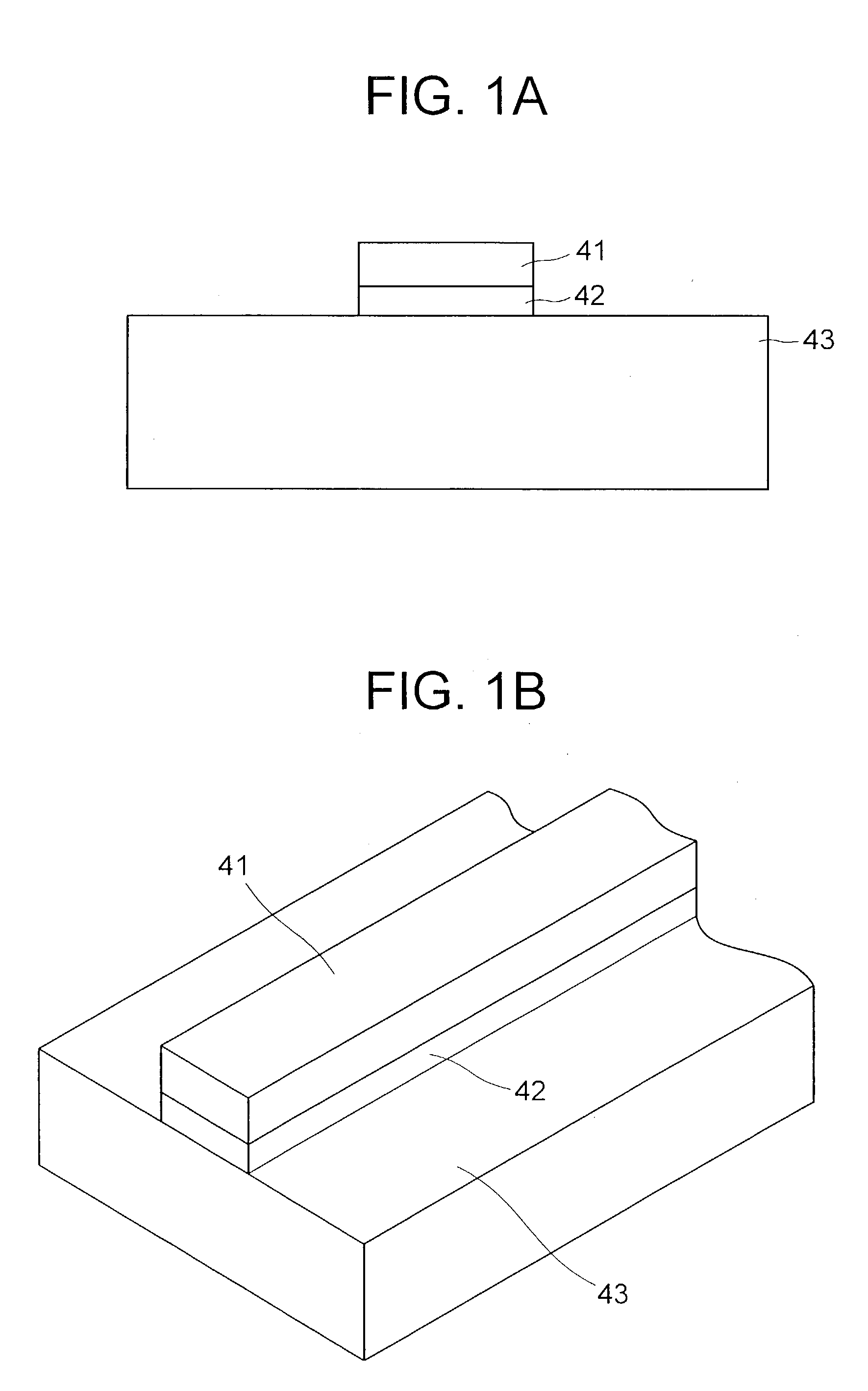
[0073] Referring to FIGS. 1A and 1B, there is shown a structure of a line device according to a first embodiment of the present invention. An interconnect line 41 of the line device is formed on a p-type or n-type semiconductor substrate 43 with an intervention of an insulator film 42. The interconnect line 41 forms a part of a power-source distribution line (referred to as simply distribution line hereinafter) which supplies power to the switching device.
[0074] The semiconductor substrate 43 may be made of any of known semiconductor materials, and may be preferably silicon in view of the feasibility of the fabrication procedure. Examples of the material for the insulator film 42 include SiO.sub.2, SiO, SiN, TaO.sub.2, TiO.sub.2, Al.sub.2O.sub.3, MgO, SrTiO.sub.3, ZrO.sub.2 and LaAlO.sub.3, but are not limited thereto. Each of these insulators may be used alone or in combination with one or more of other recited insulators. These oxide films have excellent con...
second embodiment
[0080] Second Embodiment
[0081] Next, a second embodiment will be described with reference to FIGS. 3A to 3C, wherein an insulator film such as used as a gate oxide film in a general semiconductor circuit is used in the line device to underlie the interconnect line.
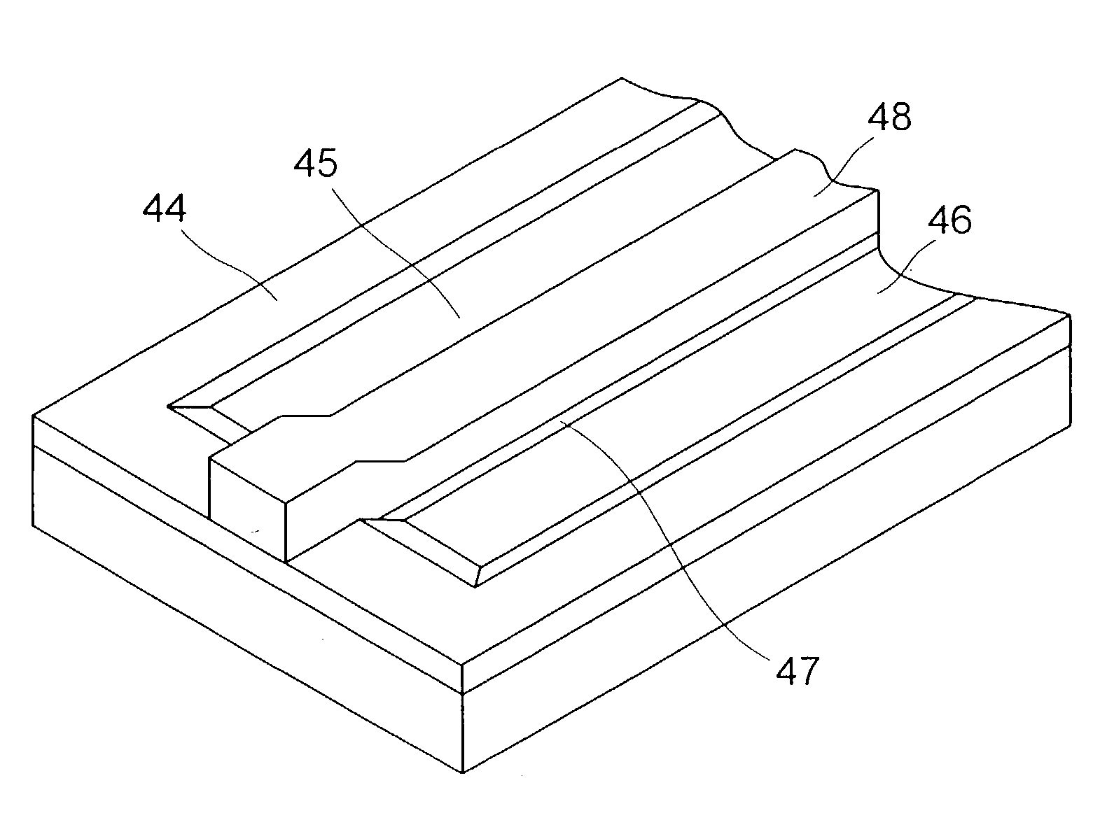
[0082] The line device shown in these drawings has a structure similar to a MOSFET, including a portion of a semiconductor (silicon) substrate 43 receiving therein diffused regions 45 and 46, an oxide film 47 formed on the semiconductor substrate 43 between the diffused regions 45 and 46 as viewed from above, and an interconnect line 48 formed on the oxide film 47. The interconnect line 48 forms a part of the distribution line to supply power source voltage.
[0083] The diffused regions 45 and 46 are received in a region encircled by a field oxide film 44, which isolates the region from other regions. The diffused regions 45 and 46 are maintained at the ground potential. The diffused regions 45 and 46 may have a conductivity...
third embodiment
[0094] Third Embodiment
[0095] Referring to FIGS. 6A, 6B and 6C, there is shown a line device according to a third embodiment of the present invention, which is similar to the second embodiment except that the resistance of the interconnect line 48 having a structure of a gate electrode line is reduced by forming a bypass line or associated interconnect line.
[0096] More specifically, the interconnect line 48 is associated with a metallic interconnect line 11 formed on an interlevel dielectric film 10 overlying the interconnect line 48. The associated interconnect line 11 has a width similar to the width of the interconnect line 48 and extends parallel thereto. The associated interconnect line 11 is connected to the interconnect line 48 via contact plugs 49 penetrating the interlevel dielectric film 10 and arranged along the interconnect line 48. In this embodiment, the interconnect line 48, contact plugs 49 and the associated interconnect line 11 form a part of the distribution line,...
PUM
 Abstract
Description
Claims
Application Information