Methods of fabricating high density mask ROM cells

a memory cell and high density technology, applied in the direction of basic electric elements, electrical equipment, semiconductor devices, etc., can solve the problems of substantial time and cost, physical limits of manufacturing processes being approached, and correction measures, although not desirable, may be necessary in conventional methods

Inactive Publication Date: 2003-11-13
MACRONIX INT CO LTD
View PDF0 Cites 13 Cited by
  • Summary
  • Abstract
  • Description
  • Claims
  • Application Information

AI Technical Summary

Benefits of technology

[0015] The above method may also further comprise the steps of adding one or more thin oxide layers and a thin polysilicon layer over the thin oxide layers. The channel between the polybars has a length and the reflective dielectric fence may be orthogonally disposed to the length of the channel. The photoresist used in the foregoing methods may be used without first applying an anti-reflective coating. The dopant used in the foregoing methods may be an N-type impurity, such as arsenic or phosphorous. The dopant of the foregoing methods may be implanted into one or more sidewalls of the trench. For example, the dopant may be implanted at an angle 15.degree. from normal, or from a vertical line extending through the semiconductor substrate. The voids formed in the foregoing methods may enhance control of the critical dimension of the sidewall.
[0018] Thus, the present invention departs from conventional methods by creating a pre-code hole pattern in a semiconductor device, the pre-code hole pattern being defined by two reflective dielectric (e.g. oxide or SOG) fences, the trench walls and base, and the channel walls. The pre-code hole pattern provides effective ion implantation into the device without being constrained by certain physical limits of optical photolithographic processes. The pre-code hole pattern also improves the removal of photoresist from areas to be implanted with ions due to reflectivity provided within the holes.

Problems solved by technology

However, as the demand for higher density memory devices increases, physical limits of the manufacturing processes are being approached.
These corrective processes can require a substantial amount of time and cost to implement, and thus, such corrective measures although not desirable may nonetheless be necessary in conventional methods.
However, as discussed above, because the densities of the components of the memory devices are approaching the physical limits of the processes used in the manufacture of the memory devices, the ion implantation process can become more difficult and time consuming.
However, as the ion implantation window size decreases, ions are implanted over a smaller area, which can result in little, if any, implantation of the sidewalls of the isolation trenches which is necessary in the creation of certain dual bit cell architectures.

Method used


Image

  • Methods of fabricating high density mask ROM cells
  • Methods of fabricating high density mask ROM cells
  • Methods of fabricating high density mask ROM cells

Examples


Embodiment Construction

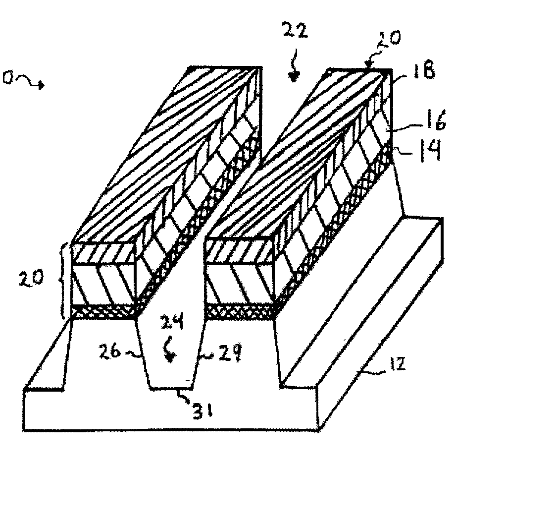
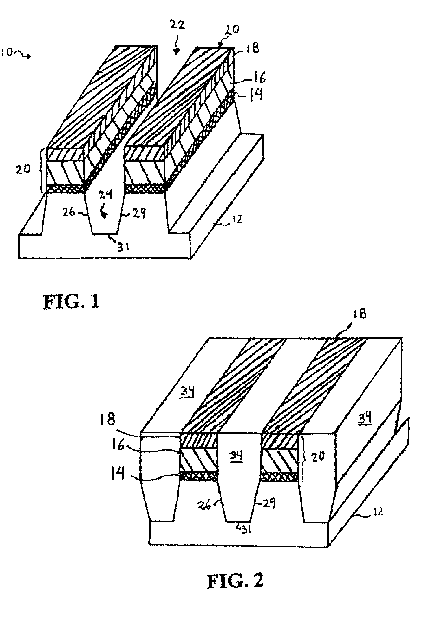
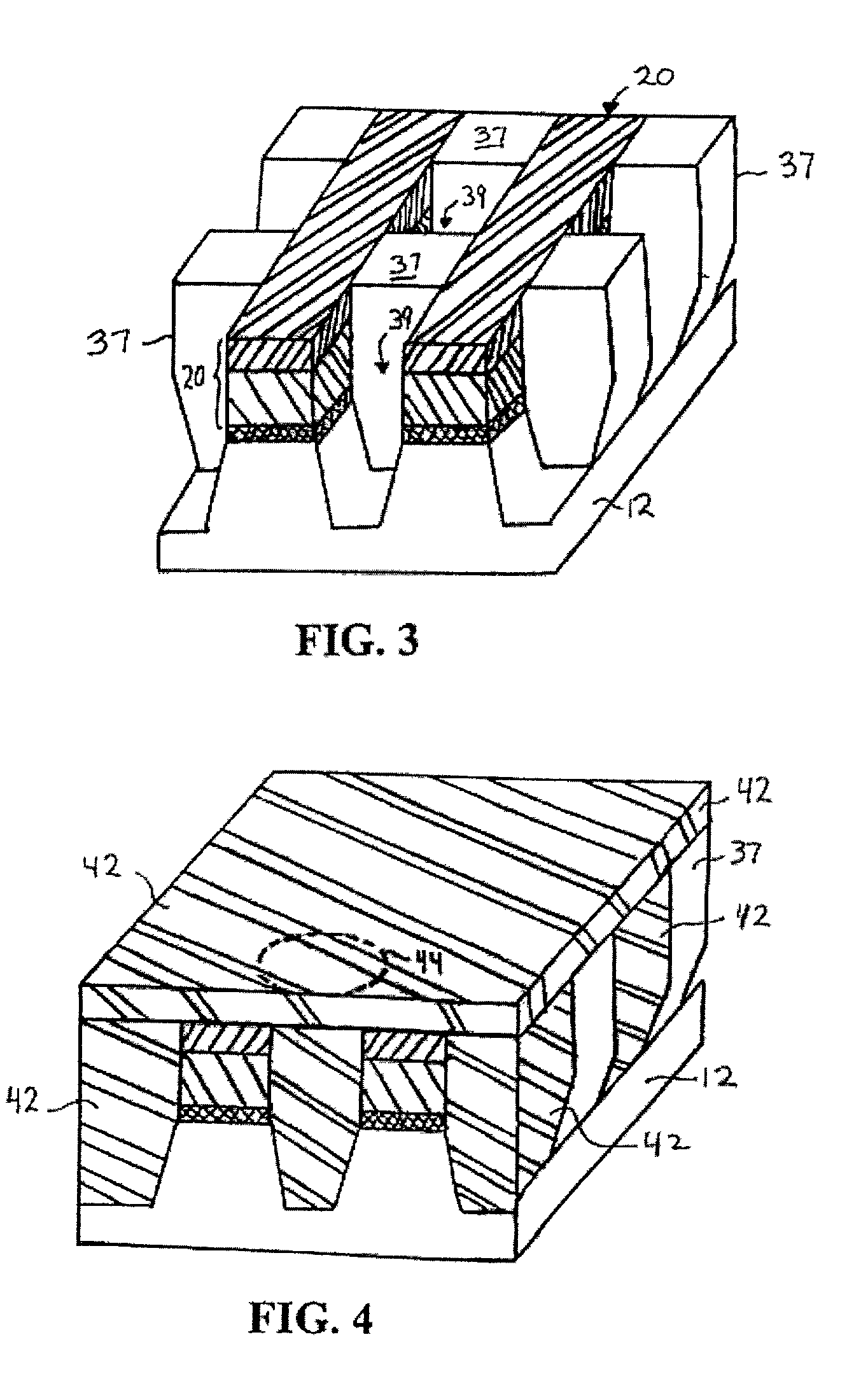
[0029] Reference will now be made in detail to the presently preferred embodiments of the invention, examples of which are illustrated in the accompanying drawings. Wherever possible, the same or similar reference numbers are used in the drawings and the description to refer to the same or like parts. It should be noted that the drawings are in greatly simplified form and are not to precise scale. In reference to the disclosure herein, for purposes of convenience and clarity only, directional terms, such as, top, bottom, left, right, up, down, above, below, beneath, rear, and front, are used with respect to the accompanying drawings. Such directional terms should not be construed to limit the scope of the invention in any manner.

[0030] Although the disclosure herein refers to certain illustrated embodiments, it is to be understood that these embodiments are presented by way of example and not by way of limitation. The intent of the following detailed description is to cover all modi...


PUM


Abstract

Methods for making integrated circuit devices, such as high density memory devices and memory devices exhibiting dual bits per cell, include forming multiple oxide fences on a semiconductor substrate between multiple polybars. The oxide fences create a hole pre-code pattern that facilitates ion implantation into trenches disposed between the polybars. The holes, or voids, formed by the oxide fences provide greater control of the critical dimension of ion implantation, for example, the critical dimension of the trench sidewalls. Semiconductor devices used in the manufacture of memory devices include the oxide fences during the manufacturing process.

Description

[0001] 1. Field of the Invention[0002] This application relates to methods of fabricating integrated circuit devices and, more particularly, to methods of fabricating high density memory cells in integrated circuit devices.[0003] 2. Description of Related Art[0004] Successful manufacture of high density memory devices, such as read only memory (ROM) devices, including EPROM, and EEPROM memory devices, is determined by the resolution capabilities of the processes used in the manufacture of such devices. For example, optical photolithographic processes have been developed to utilize smaller wavelengths of light to pattern the components of the semiconductor memory devices. The smaller wavelengths of light provide finer precision in exposing regions of the memory devices to the light. Currently, lasers are being employed in the processing of these memory devices.[0005] However, as the demand for higher density memory devices increases, physical limits of the manufacturing processes are...

Claims


Application Information

Patent Timeline
Patent Type & Authority Applications(United States)
IPC IPC(8): H01L21/336H01L21/8236H01L21/8246H01L27/112
CPCH01L27/112H01L27/1126H01L27/11253H10B20/38H10B20/383H10B20/00
Inventor CHANG, CHING-YU
Owner MACRONIX INT CO LTD
Why Eureka
Try Eureka