Scaleable microprocessor architecture

a microprocessor and architecture technology, applied in the direction of next instruction address formation, program control, instruments, etc., can solve the problems of increasing the complexity of the instruction set is still quite large, and the complexity of the instruction set is still large, so as to achieve the effect of rapid and reliable execution

Inactive Publication Date: 2003-11-13
TING CHEN HANSON
View PDF14 Cites 12 Cited by
  • Summary
  • Abstract
  • Description
  • Claims
  • Application Information

AI Technical Summary

Benefits of technology

0016] It is the object of this invention to provide a microprocessor architecture based on a dual stack central processing unit (CPU) with a set of 20 simple, efficient and orthogonal instructions. An orthogonal instruction set contains instructions with minimal redundant and overlapped functions. These instructions can be encoded in 5-bit fields of a program word. Using 5-bit instructions, it is possible to construct microprocessors of word size scaleable from 15 bits up, including but not limited to 16, 24, 32, and 64 bits. Since all these microprocessors execute an identical instruction set, they can share subroutine libraries, software development tools, and operating systems.
0017] It is another object of this invention to provide a series of microprocessors with dual stack CPU and 5-bit instructions, which latch the appropriate data into all the registers and stacks on the rising edge of a master clock. Such synchronous architecture ensures that all instructions are executed quickly and reliably in a single clock cycle from a single phase master clock.
0018] It is a further object of this invention to provide microprocessor systems, comprising a central processing unit using said instruction set, a memory device, and a plurality of I/O devices, in a single integrated circuit. Such microprocessor systems form the cores of System-on-a-Chiip (SOC) integrated circuits.
0019] The attainment of these and related objects may be achieved through use of a novel design herein disclosed. In accordance with one aspect of the invention, a microprocessor system in accordance with this invention has a central processing unit CPU, a means to connect to an external reset signal RST, a means to connect to a master clock signal CLK, a memory device to store program words and data, a means to connect said memory device to said CPU in the form of an address bus, a data bus and a plurality of control signals, and a means to connect to external I/O devices like a terminal. Said address bus and said data bus have the same width N as the word size of the microprocessor, from 15 bits up, including but not limited to 16,

Problems solved by technology

The instruction set becomes complicated by large number of different memory accessing modes.
In the mean time, families of RISC computers had also evolved with many added functions and circuitry, to the point that newer RISC computers are as complicated as the newer CISC computers.
However, the latest designs by Moore (1995-1998) limited the machine instructions to a set of about 200 instructions, and encoded these instructions in 8-bit byte code.
This instruction set was still fairly complicated like the CISC computers and required very substanti

Method used


Image

  • Scaleable microprocessor architecture
  • Scaleable microprocessor architecture
  • Scaleable microprocessor architecture

Examples


Embodiment Construction

, taken together with the drawings.

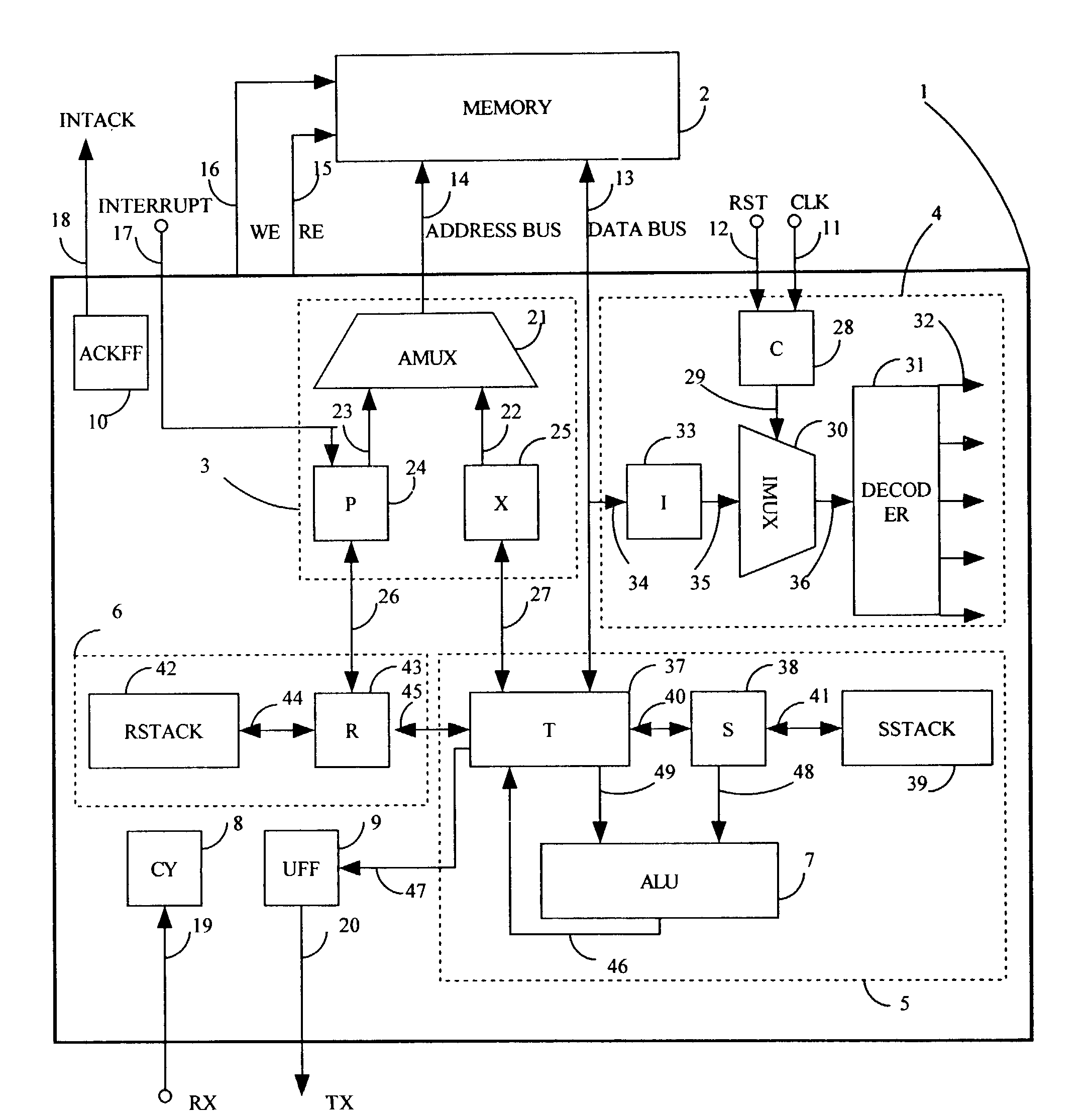
[0045] FIG. 1 is an overall block diagram of the scaleable microprocessor in accordance with the invention.

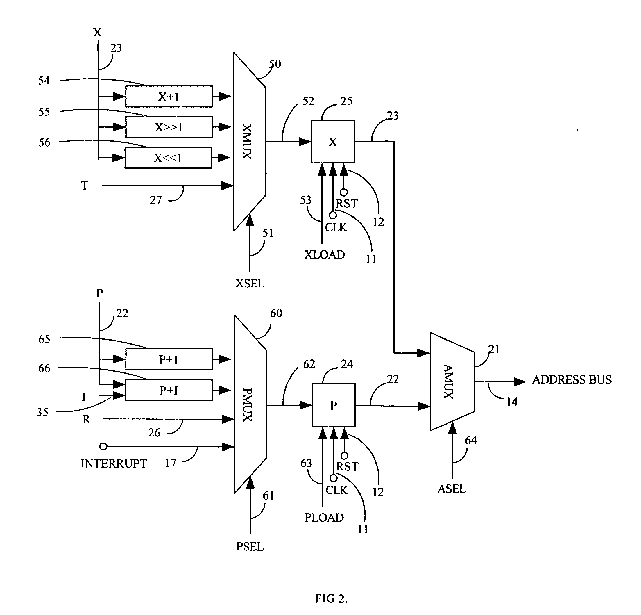
[0046] FIG. 2 is a block diagram of Address Processing Unit.

[0047] FIG. 3 is a block diagram of Instruction Sequencing Unit.

[0048] FIG. 4 is a timing diagram of program execution after reset RST is released.

[0049] FIG. 5 is a timing diagram of a branch instruction.

[0050] FIG. 6 is a block diagram of Data Processing Unit.

[0051] FIG. 7 is a block diagram of Address Storage Unit.

[0052] FIG. 8 is a block diagram of T and X registers to support MUL instruction.

[0053] FIG. 9 is a block diagram of T and X registers to support DIV instruction.

[0054] FIG. 10 is a block diagram of CY and UFF flip-flops to support a serial I / O port with SHR instruction.

[0055] FIG. 11 is a block diagram of INTFF and ACKFF flip-flops to service real time interrupts.

DESCRIPTION--OVERVIEW

[0056] The scaleable microprocessor architecture of this invention is a new way in micro...


PUM


Abstract

A scaleable microprocessor architecture has an efficient and orthogonal instruction set of 20 basic instructions, and a scaleable program word size from 15 bits up, including but not limited to 16, 24, 32, and 64 bits. As many instructions are packed into a single program word as allowed by the size of a program word. An integral return stack is used for nested subroutine calls and returns. An integral data stack is also used to pass parameters among nested subroutines. The simplified instruction set and the dual stack architecture make it possible to execute all instructions in a single clock cycle from a single phase master clock. Additional instructions can be added to facilitate accessing arrays in memory, for multiplication and division of integers, for real time interrupts, and to support an UART I/O device. This scaleable microprocessor architecture greatly increases code density and processing speed while decreasing significantly silicon area and power consumption. It is most suitable to serve as microprocessor cores in System-on-a-Chip (SOC) integrated circuits.

Description

[0001] 1. Field of the Invention[0002] The present invention relates generally to a microprocessor architecture which has a simple, efficient, and orthogonal instruction set and can be implemented in program word sizes ranging from 15 bits up to 64 bits, and such scaleable microprocessors are most suitable to be used as cores of System-on-a-Chip (SOC) integrated circuits.[0003] 2. Description of the Prior Art[0004] Currently the prevailing computer and microprocessor architectures are all register-centric, in that the central processing unit CPU in a microprocessor contains a large set of registers. Data from memory and I / O devices are first read into the registers to be processed by the CPU. Results are then written out from the registers to memory or to I / O devices. Complicated Instruction Set Computers (CISC) like Intel 80.times.86 and Motorola 680.times.0 have instructions which can read data from memory, using many different memory accessing modes, and also operate on the data ...

Claims


Application Information

Patent Timeline
IPC IPC(8): G06F9/30G06F9/302G06F9/32G06F9/38
CPCG06F9/3001G06F9/321G06F9/38G06F9/30127G06F9/3824G06F9/3853G06F9/3806
Inventor TING, CHEN-HANSON
Owner TING CHEN HANSON
Why Eureka
Try Eureka