Semiconductor device

a technology of semiconductors and devices, applied in the direction of semiconductor devices, basic electric elements, electrical equipment, etc., can solve the problems of reducing the breakdown voltage of the device, increasing the on-state resistance ron of the device,

Inactive Publication Date: 2003-12-11
KK TOSHIBA
View PDF5 Cites 61 Cited by
  • Summary
  • Abstract
  • Description
  • Claims
  • Application Information

AI Technical Summary

Benefits of technology

[0003] The present invention relates to a semiconductor device and, more particularly, to a semiconductor device having a power MOSFET (Metal Oxide Semiconductor Field Effect Transistor) structure.

Problems solved by technology

However, when the impurity concentration of the Njfet region 90 is lowered to make the Njfet region 90 easily depleted, a problem occurs such that an ON-state resistance Ron of the device increases and, as a result, a breakdown voltage of the device decreases.

Method used


Image

  • Semiconductor device
  • Semiconductor device
  • Semiconductor device

Examples


first embodiment

[0036] (1) First Embodiment

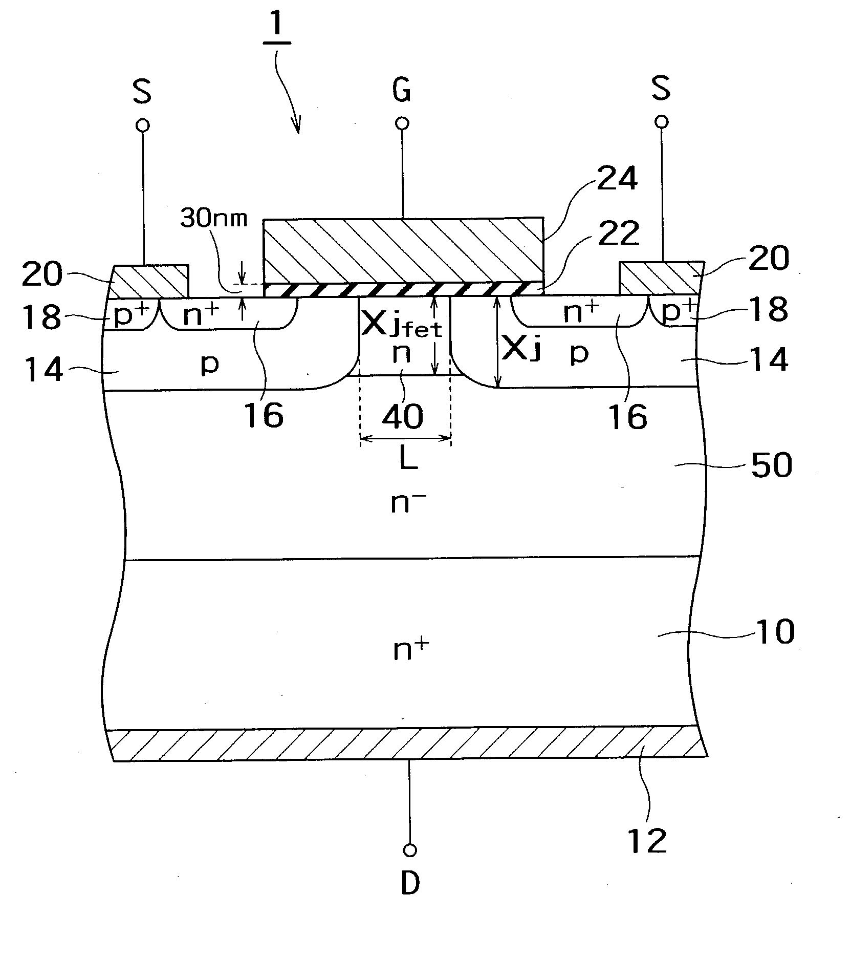
[0037] FIG. 1 is a schematic cross section showing a first embodiment of a semiconductor device according to the invention. The semiconductor device of the present embodiment is characterized in that an Njfet region 40 is formed in a narrow width at a high concentration. The structure of the semiconductor device of the embodiment will be described in more detail hereinbelow.

[0038] A power MOSFET 1 shown in FIG. 1 is a power MOSFET of a vertical type to which the invention is applied, and includes an n.sup.+ type low-resistance semiconductor substrate 10, a drain electrode 12, an n.sup.- type high-resistance epitaxial layer 50, a p type base layer 14, an n.sup.+ type source layer 16, the Njfet region 40, a gate electrode 24, and a source electrode 20.

[0039] The drain electrode 12 is provided on one of the surfaces (under face in FIG. 1) of the n.sup.+ type low-resistance semiconductor substrate 10, and the n.sup.- type high-resistance epitaxial layer 50 is ...

second embodiment

[0045] (2) Second Embodiment

[0046] FIG. 4 is a schematic cross section showing a second embodiment of a semiconductor device according to the invention. As obviously understood from comparison with FIG. 1, a power MOSFET 3 of the second embodiment is characterized in that a gate insulating film 23 is formed so as to be thicker in a region facing the Njfet region 40 as well as in that the Njfet region 40 is formed in narrow width and at high concentration. More specifically, a portion 23a of the gate insulating film 23 facing the Njfet region 40 has a thickness of about 90 nm whereas the other portion of the gate insulating film 23 is formed to have a thickness of about 30 nm. By the configuration, in the region facing the Njfet region 40, a gate electrode 25 can be further isolated from the Njfet region 40.

[0047] Since the Njfet region 40 is formed in narrow width and at high concentration, at the time of depleting the Njfet region 40, depletion from the p type base layer 14 becomes...

third embodiment

[0049] (3) Third Embodiment

[0050] FIG. 5 is a schematic cross section showing a third embodiment of a semiconductor device according to the invention. As obviously understood by comparison with FIG. 1, a power MOSFET 5 of the third embodiment is characterized in that a portion facing the Njfet region 40 in the gate electrode 28 is selectively removed.

[0051] By employing the structure in which the gate electrode 28 is divided as described above, the width L of the Njfet region 40 can be further narrowed, so that the gate-drain capacitance Q.sub.gd is further reduced and operation speed of the device is further increased. By implanting n-type impurities using the gate electrode 28 in the divisional structure as a mask, the Njfet region 40 can be formed in a self-aligned manner.

[0052] FIGS. 6 and 7 are diagrams for explaining reduction in the gate-drain capacitance Q.sub.gd according to the third embodiment. FIG. 6 shows electron density in the conventional power MOSFET 100 illustrated...


PUM


Abstract

A semiconductor device includes: a semiconductor substrate, at least a surface portion thereof serving as a low-resistance drain layer of a first conductivity type; a first main electrode connected to the low-resistance drain layer; a high-resistance epitaxial layer of a second-conductivity type formed on the low-resistance drain layer; a second-conductivity type base layer selectively formed on the high-resistance epitaxial layer; a first-conductivity type source layer selectively formed in a surface portion of the second-conductivity type base layer; a trench formed in a region sandwiched by the second-conductivity type base layers with a depth extending from the surface of the high-resistance epitaxial layer to the semiconductor substrate; a jfet layer of the first conductivity type formed on side walls of the trench; an insulating layer formed in the trench; an LDD layer of the first-conductivity type formed in a surface portion of the second-conductivity type base layer so as to be connected to the first-conductivity type jfet layer around a top face of the trench; a control electrode formed above the semiconductor substrate so as to be divided into a plurality of parts, and formed on a gate insulating film formed on a part of the surface of the LDD layer, on surfaces of end parts of the first-conductivity type source layer facing each other across the trench, and on a region of the surface of the second-conductivity type base layer sandwiched by the LDD layer and the first-conductivity type source layer; and a second main electrode in ohmic contact with the first-conductivity type source layer and the second-conductivity type base layer so as to sandwich the control electrode.

Description

[0001] This application claims benefit of priority under 35USC .sctn.119 to Japanese patent application No. 2002-94361, filed on Mar. 29, 2002, the contents of which are incorporated by reference herein.[0002] 1. Field of the Invention[0003] The present invention relates to a semiconductor device and, more particularly, to a semiconductor device having a power MOSFET (Metal Oxide Semiconductor Field Effect Transistor) structure.[0004] 2. Related Background Art[0005] In recent years, demand for a power MOSFET has been rapidly increasing in the field of a switching power source of heavy current and high breakdown voltage and, in addition, in the field of switching elements for energy saving of mobile communication devices such as a notebook-sized PC (Personal Computer). Since the power MOSFET is often used for a power management circuit, a safety circuit of a lithium ion battery, and the like in these fields, driving with a lower voltage so that the device can be directly driven with ...

Claims


Application Information

Patent Timeline
Patent Type & Authority Applications(United States)
IPC IPC(8): H01L21/265H01L21/336H01L29/06H01L29/08H01L29/10H01L29/40H01L29/423H01L29/78
CPCH01L21/26586H01L29/0653H01L29/0696H01L29/0847H01L29/1095H01L29/402H01L29/7809H01L29/42368H01L29/42376H01L29/4238H01L29/66712H01L29/7802H01L29/407H01L29/0878
Inventor ONO, SYOTAROYAMAGUCHI, YOSHIHIROKAWAGUCHI, YUSUKENAKAMURA, KAZUTOSHIYASUHARA, NORIOMATSUSHITA, KENICHIHODAMA, SHINICHINAKAGAWA, AKIO
Owner KK TOSHIBA
Why Eureka
Try Eureka