

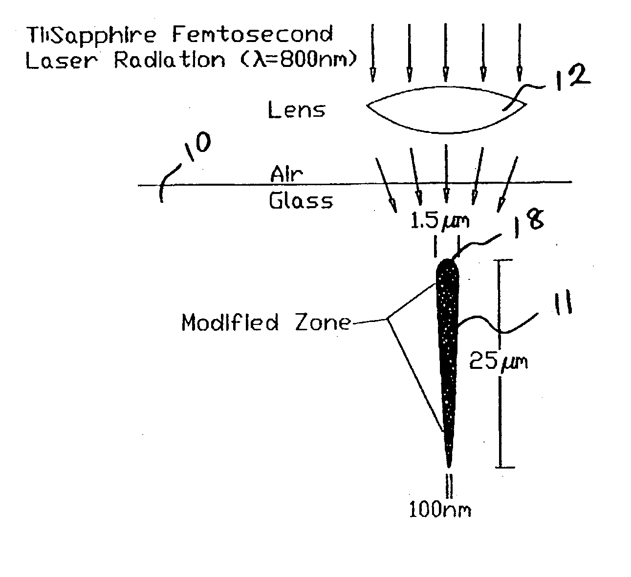
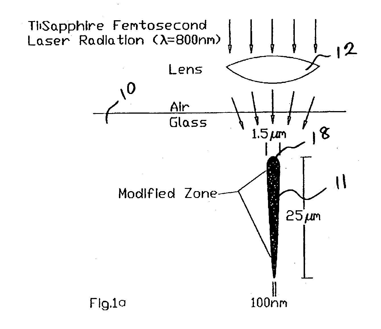
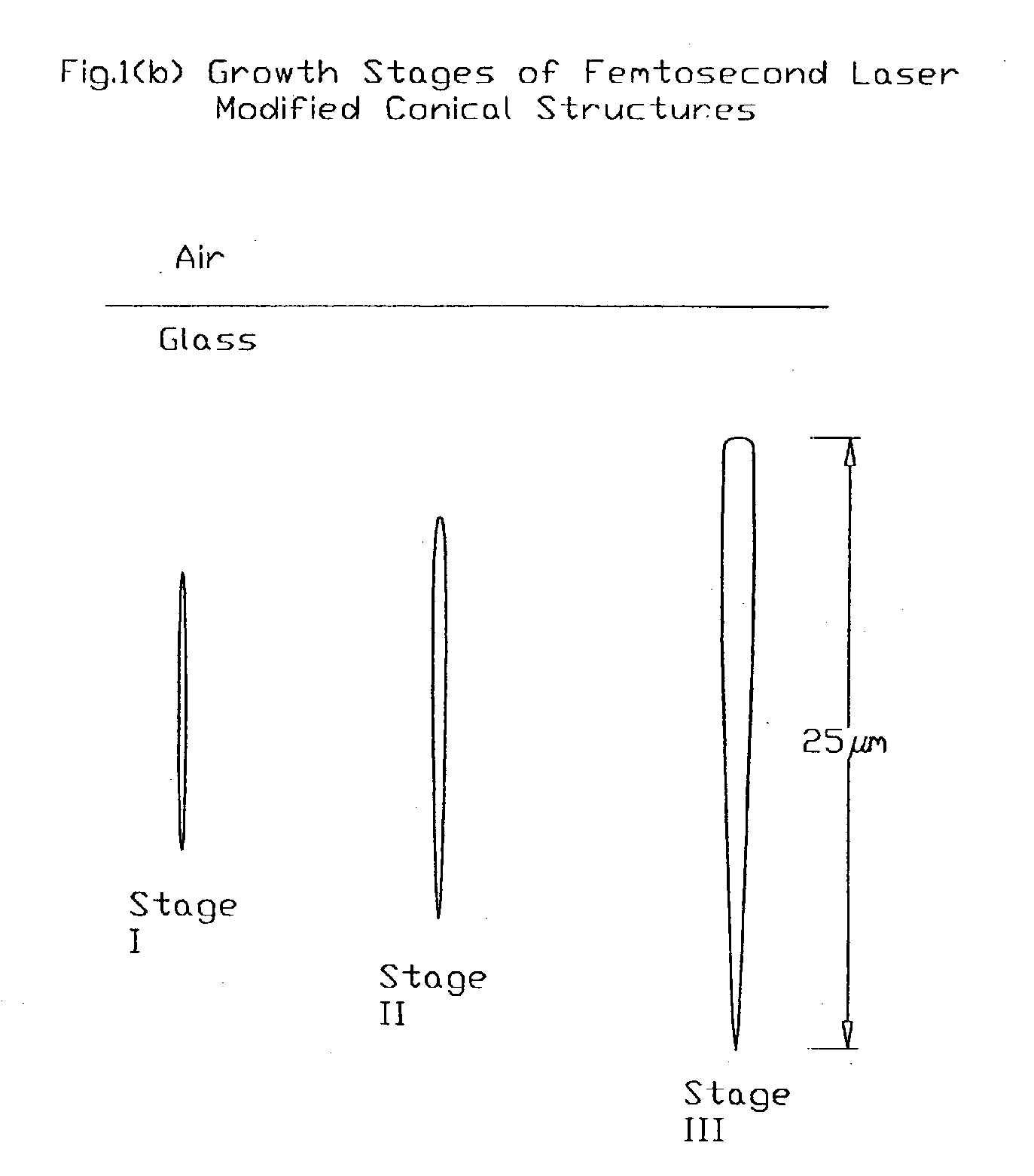
Method of fabricating sub-micron structures in transparent dielectric materials
a dielectric material and submicron structure technology, applied in the field of fabricating submicron structures in transparent dielectric materials, can solve the problems of high damage to the modified silica zone, inability to form low-loss optical waveguides, and severe restriction of the distance between the lens and the irradiated zone, so as to achieve different symmetry, increase the width, and reduce the effect of width
- Summary
- Abstract
- Description
- Claims
- Application Information
AI Technical Summary
Benefits of technology
Problems solved by technology
Method used
Image

Examples
example 2
[0087] Microfluidic Applications on a Silica Chip
[0088] The method in accordance with the invention permits the production of precise channels, which can be tapered and formed into complicated patterns such as mixing chambers for chemistry on a chip experiments.
[0089] The value of these narrow channels for chemistry on a chip experiments is enhanced since with each channel there is an adjoining optical waveguide, which can couple light into or out of the channel. One could also use arrays of micron-sized holes to trap very small droplets of liquid for analysis.
[0090] It is also possible to partially coat the interior of the channels / holes with metal. The metal is then removed everywhere except in the channels / holes by polishing. Laser radiation delivered through the waveguides attached to the channels / holes can be absorbed by the metal to control the temperature of samples placed in such channels / holes. The laser radiation can also be used heat the samples sufficiently rapidly to ej...
example 3
[0091] Biological Sensing Applications on a Chip
[0092] Very small volumes of biological material can be inserted into the narrow channels where it can be interrogated by light traveling in the waveguide adjoining the channel.
[0093] There are also biological sensor applications for holes and their vertically connected waveguides. For example, biological specimens could be inserted into the holes. An entire array of holes could then be irradiated with UV light and the fluorescence from each specimen could be guided by its own waveguide for selective detection. Alternatively holes containing a sample could be individually irradiated or sampled through its own waveguide.
[0094] It is also possible to use light traveling in a horizontal waveguide, which has no adjoining channel but instead interfaces with a series of holes, to simultaneously irradiate material contained in all of the holes. Light emanating from each hole e.g. fluorescence, can be detected using the dedicated vertical wave...
example 4
[0095] Insertion of Materials between Interconnected Waveguides for Telecom Applications
[0096] It will be appreciated that the method of the invention makes it possible to create a hole (FIG. 3) at the termination of a waveguide i.e. at the glass / air boundary. The hole diameter can have approximately the same dimensions as the waveguide. Arrays of such waveguides can be written inside a block of dielectric and terminated in such holes. The holes can then be filled with material which could alter the intensity, polarization or other properties of the light propagating through the holes to interconnect with an external set of waveguides butted to the holes.
PUM
| Property | Measurement | Unit |
|---|---|---|
| diameter | aaaaa | aaaaa |
| diameter | aaaaa | aaaaa |
| thickness | aaaaa | aaaaa |
Abstract
Description
Claims
Application Information