Electronic component package and method of manufacturing same

a technology of electronic components and components, applied in the direction of electrical equipment, semiconductor devices, semiconductor/solid-state device details, etc., can solve the problems of reducing the peel strength of the fusion-welding layer, reducing and easy formation of pinholes, so as to prevent the change of fusion welding and suppress the formation of voids in the intermetallic compound during fusion welding. , the effect of improving the stability of the fusion welding

Inactive Publication Date: 2004-02-05
SUMITOMO SPECIAL METAL CO LTD +1
View PDF2 Cites 13 Cited by
  • Summary
  • Abstract
  • Description
  • Claims
  • Application Information

AI Technical Summary

Benefits of technology

0037] In the fusion welding of the package assembly, merely melting and solidifying the soldering material is insufficient and it is required that the intermetallic compound layers be grown to the predetermined area ratio by diffusion. To realize fusion welding accompanying adequate growth of such an intermetallic compound the package assembly is usually held at a temperature about 50 to about 250.degree. C. higher than the melting point of the soldering material for about 300 to about 1500 sec. However, some types of electronic components may be deteriorated in their characteristics when they are held in a high-temperature condition for a prolonged time. In such a case it is desirable to employ such a process including: holding the package assembly at a temperature about 10 to about 30.degree. C. higher than the melting point of the soldering material for about 10 to about 30 sec to melt the soldering material: after having allowed the molten soldering material to contact the surfaces of the metal layers sufficiently, rapidly lowering the temperature to a package-holding temperature ranging from a point about 50.degree. C. lower than the melting point of the soldering material to a point just short of the melting point; and holding the package assembly at the package-holding temperature for about 2 to about 20 hr to grow the intermetallic compound. This process makes it possible to obtain the intended fusion-welding layer 20 without deteriorating the characteristics of the electronic component contained in the package. It is to be noted that the melting point of a solder alloy such as an Sn-based solder alloy is equivalent to the eutectic temperature of the solder alloy.
0038] In the fusion welding it is sufficient to heat the package assembly with the lid member 8 preferably positioned under the case 1. It is, however, desirable that the package assembly be intentionally pressurized so that the case 1 and the lid member 8 are pressed against each other. By so doing, the formation of voids in the intermetallic compound during the fusion welding can be suppressed, so that the stability of fusion welding can be improved. It is possible to employ a pressurizing method such as to place a weight on the package assembly via a presser plate formed of a material that does not react with the surface of the package assembly, e.g. a ceramic material, or a pressurizing method such as to bias the presser plate against the package assembly by means of a spring. The pressure to be applied usually ranges from about 2.times.10.sup.-4 to about 1.times.10.sup.-2 N / mm.sup.2.
0039] Usually, heating for the fusion welding is performed in a vacuum or in an inert gas atmosphere. The fusion welding in a vacuum or an inert gas atmosphere such as nitrogen gas makes it possible to prevent the electronic component from being oxidized by heating as well as to form an electronic component containing space provided with a vacuum or an inert gas atmosphere after the fusion welding. Thus, the electronic component can be prevented from changing with time. Particularly where an oscillator such as a quartz crystal oscillator is contained in the package, it is desirable from the viewpoint of improvement in resonance characteristic that the fusion welding be performed under vacuum.

Problems solved by technology

If the area ratio of the first and second intermetallic compound layers is less than 25%, the area of the first and second intermetallic compound layers of uneven shape is so small that the soldering material layer becomes re-melted in an extended region between the first and second intermetallic compound layers when re-heated, resulting in easy formation of such defects as pinholes.
On the other hand, if the ratio is more than 98%, voids are likely to result during the irregular growth of the intermetallic compound layers so that cracks are formed as extending from such voids in the intermetallic compound layers, resulting in the package having lowered airtightness as in the former case.
Further, the amount of the soldering material sandwiched between the first and second intermetallic compound layers is reduced and, hence, the fusion-welding layer, as a whole, becomes brittle and exhibits a lowered peel strength.

Method used


Image

  • Electronic component package and method of manufacturing same
  • Electronic component package and method of manufacturing same

Examples


Embodiment Construction

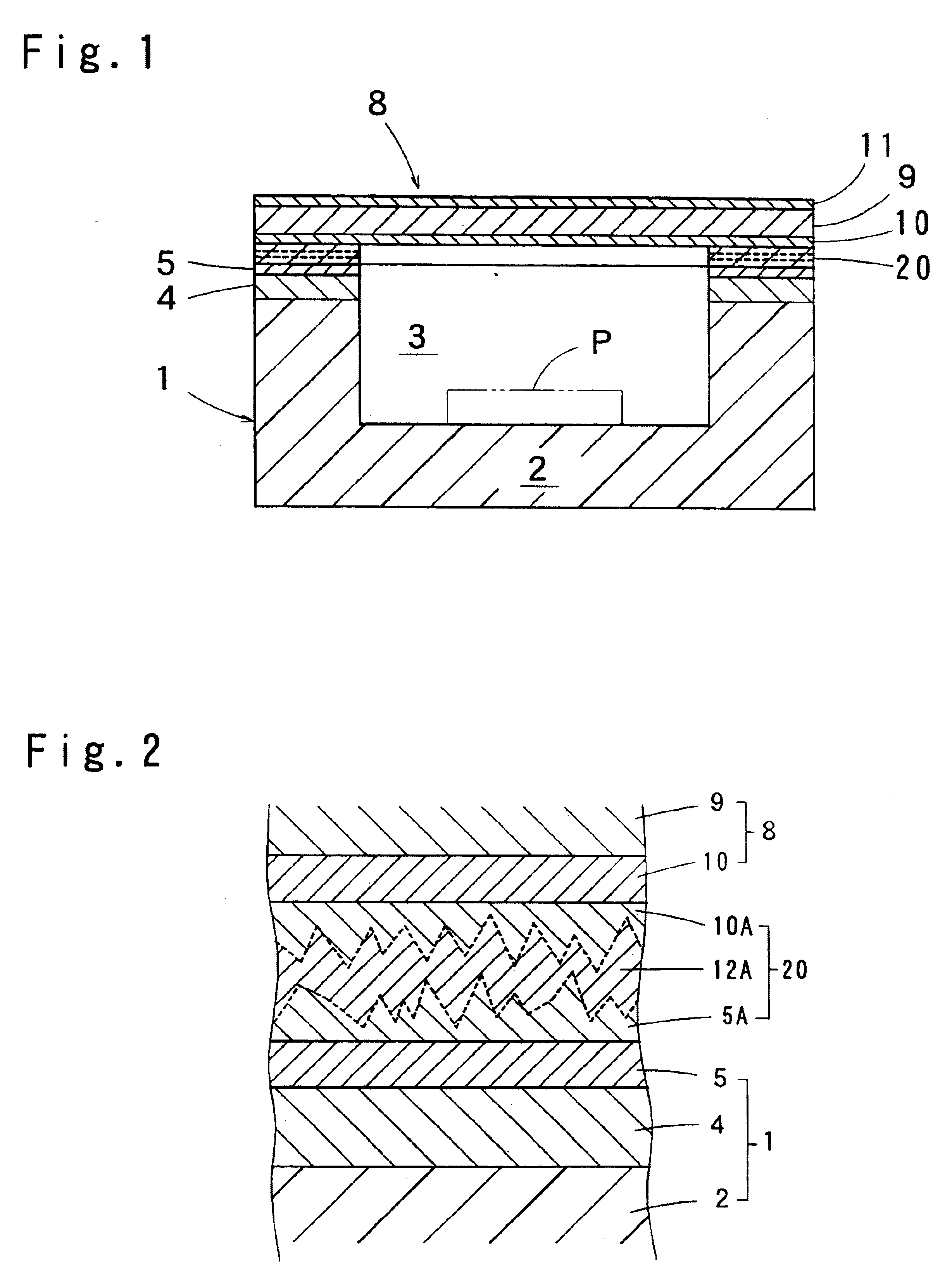
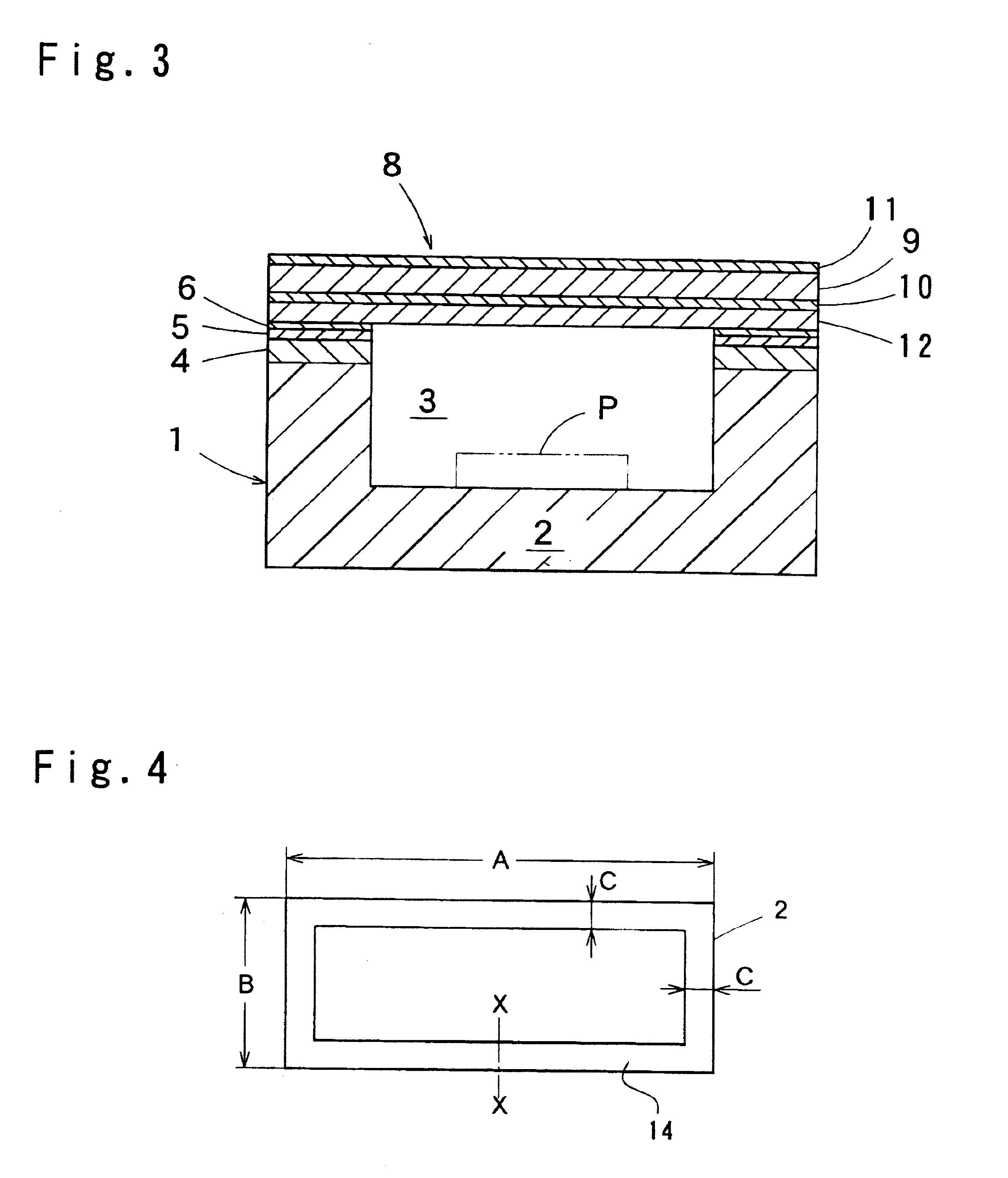
[0041] Cases were provided each having a W metallized layer (thickness: 30 .mu.m), an Ni layer (thickness: 15 .mu.m) and an Au layer (thickness: 1 .mu.m), which had been stacked in that order on a peripheral edge surface of a case body formed of a ceramic at the cavity open side, the peripheral edge surface surrounding the opening of a cavity defined in the case body. Lid members, which were separately provided, were each superposed on the Au layer side of each case via a soldering material to give package assemblies. As shown in FIG. 4, each case was sized in top plan as follows: length A=4.1 mm, overall width B=2.6 mm, and width C=0.35 mm, width C which is the width of peripheral edge surface 14 on the cavity open side from the outer periphery of the case to the inner periphery of the cavity portion. The planar size of each lid member was substantially equal to that of each case.

[0042] Each lid member had been manufactured through a process including: pressure-welding an Ni sheet ...


PUM


Abstract

An electronic component package according to the present invention includes a case (1) having a cavity portion containing an electronic component therein, and a lid member (8) fusion-welded to the case (1) via a fusion-welding layer (20) to close the cavity portion hermetically. The case (1) has a first metal layer (5) laminated on the case (1) in a manner to be exposed on the cavity open side. The lid member (8) has a core portion (9), and a second metal layer (10) laminated on a side of the core portion (9) facing the case (1). The fusion-welding layer (20) has a soldering material layer (12A) formed of a soldering material, and first and second intermetallic compound layers (5A) and (10A), respectively, formed on opposite sides of the soldering material layer (12A) as a result of diffusion of a major component of the soldering material into the first metal layer (5) and the second metal layer (10). The ratio of the area of the first and second intermetallic compound layers (5A) and (10A) in a longitudinal section of the fusion-welding layer (20) to the area of the longitudinal section of the fusion-welding layer (20) is in a range of from 25 to 98%. This package maintains superior airtightness even when exposed to a high-temperature atmosphere, which is higher than the melting point of the soldering material.

Description

[0001] The present invention relates to an electronic component package containing an electronic component therein.[0002] Various electronic components, such as semiconductor devices, quartz crystal oscillators and piezoelectric vibrators, are often contained in respective electronic component packages in order for the electronic components contained therein to be protected from external environment.[0003] As disclosed in Japanese Patent Laid-Open Gazettes Nos. 2000-58687 and 2000-164746, there are known electronic component packages of the type comprising a case formed to define a cavity that opens at the upper side of the case for containing an electronic component, and a lid member fusion-welded to a peripheral edge surface of the case surrounding the opening defined at the upper side of the case with a soldering material in order to close the cavity hermetically. The cavity defines an electronic component containing space shutting out the outside world when the lid member is fus...

Claims


Application Information

Patent Timeline
Patent Type & Authority Applications(United States)
IPC IPC(8): H01L23/04H01L23/10
CPCH01L23/04H01L2924/16195H01L2924/01079H01L23/10H01L23/02
Inventor SHIOMI, KAZUHIROISHIO, MASAAKIIIZUKA, MINORUOGASAWARA, YOSHIKIYO
Owner SUMITOMO SPECIAL METAL CO LTD
Why Eureka
Try Eureka