

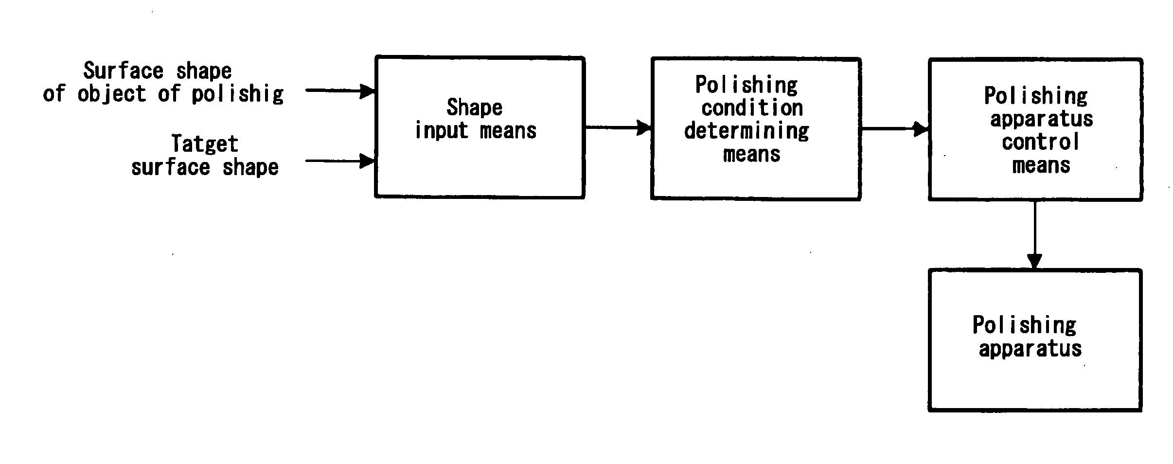
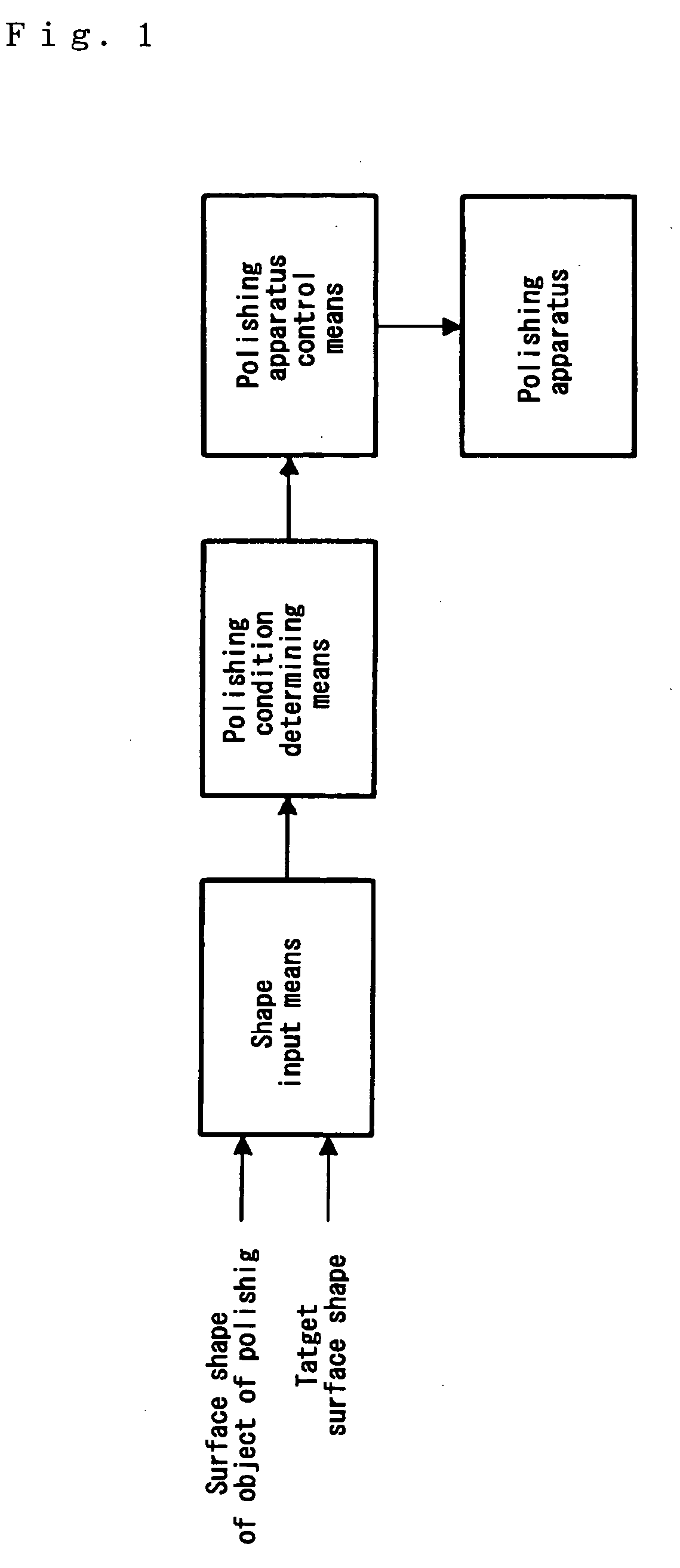
Working shape prediction method, working requirement determination method, working method, working system, method of manufacturing semiconductor device, computer program, and computer program storage medium
a technology of working shape and working requirement, applied in semiconductor/solid-state device testing/measurement, manufacturing tools, lapping machines, etc., can solve the problems of wiring interruption, drop in electrical capacitance, and individual processes involved in semiconductor manufacturing processes. to achieve the effect of accurate working conditions
- Summary
- Abstract
- Description
- Claims
- Application Information
AI Technical Summary
Benefits of technology
Problems solved by technology
Method used
Image

Examples
embodiment 1
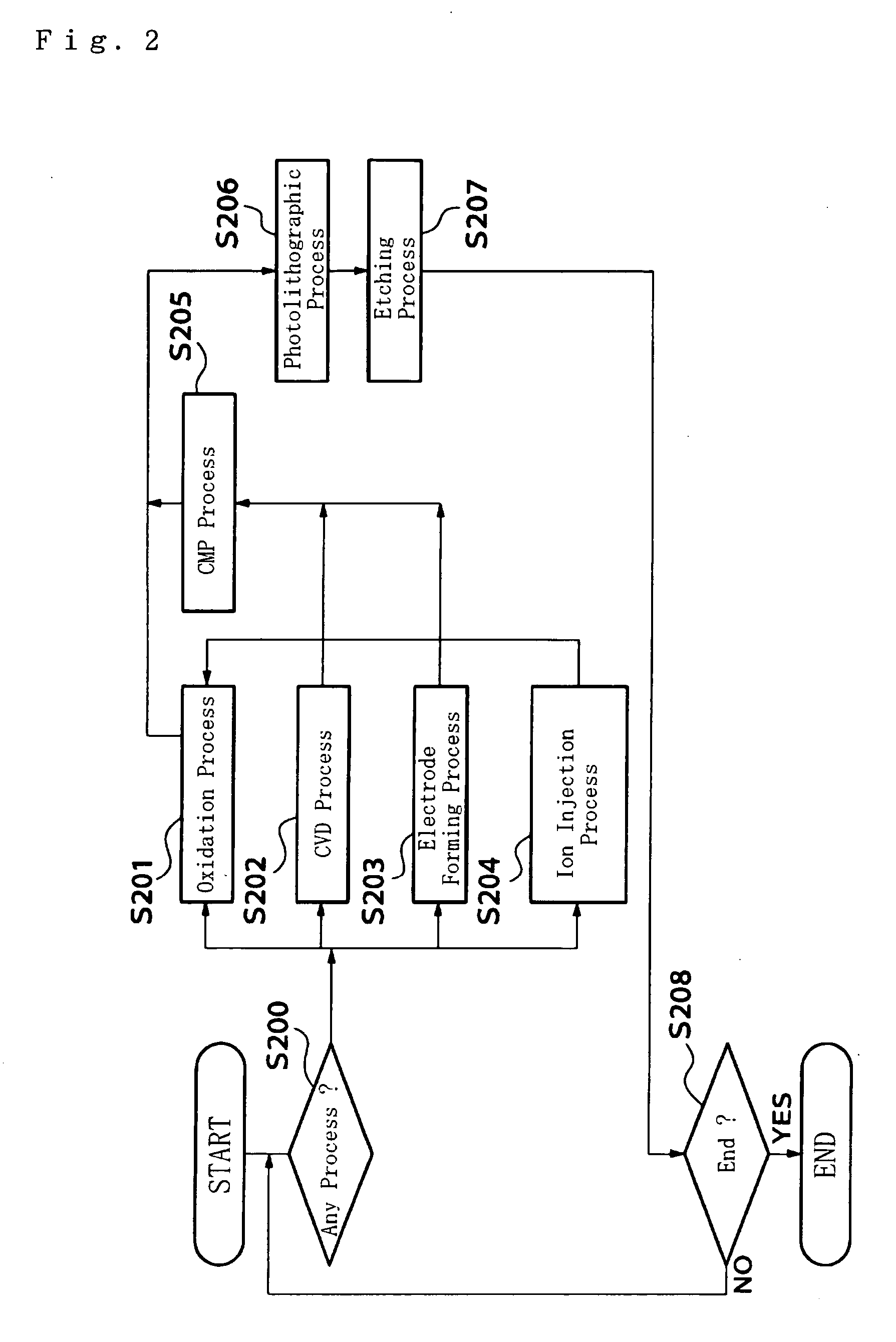
[0126] The polishing of a wafer with a diameter of 200 mm in which a Cu pattern was formed inside was performed using a polishing apparatus in which the polishing pad was smaller than the wafer. This polishing was performed using an annular polishing pad with an external diameter of 150 mm and an internal diameter of 50 mm under the following conditions: head rpm 400 rpm, wafer rpm 200 rpm, polishing time 60 sec, slurry 100 ml (RD98052, FUJIMI Incorporated). These are the same conditions as in The initial film thickness of the wafer showed an extremely high uniformity. The polishing conditions for realizing polishing that would produce a flat worked shape in one step using this wafer were determined by trial and error. 20 wafers were required in order to determine these conditions. The time required in order to determine the conditions was 4 hours.
PUM
 Abstract
Description
Claims
Application Information