Optical waveguide coupler circuit device

a technology of optical waveguide and coupler, which is applied in the direction of optical waveguide light guide, instruments, optics, etc., can solve the problems of negative value, loss characteristics dependent of polarization (pdl) are rather worse, and the temperature range under which the normal operation can be limited

Inactive Publication Date: 2004-04-08
NITTA CORP
View PDF7 Cites 13 Cited by
  • Summary
  • Abstract
  • Description
  • Claims
  • Application Information

AI Technical Summary

Benefits of technology

[0015] Accordingly, the object of the present invention is to provide a Mach-Zehnder interferometer-based polymeric waveguide circuit unaffected with the change of polarization and ambient temperature which is obtainable by arranging waveguides on a silicon or quartz substrate using conventional IC technology, while maintaining the advantage of low production cost which is the most important impetus for the introduction of polymeric optical waveguide circuits.
[0016] In a polymeric optical waveguide coupler circuit, according to a application, the optical waveguide coupler circuit give priority to a characteristics dependent of temperature or give priority to both the characteristics dependent of temperature and polarization. Inventors of this application previously proposed a polymeric optical waveguide coupler circuit which could suppress the fluctuation of output which is produced as a result of change of ambient temperature, taking into account of the characteristics independent of temperature.

Problems solved by technology

However, because the 2.times.2N splitter shown in FIG. 2 includes the waveguides made from a polymer, its optical characteristics are apt to vary in the presence of changes of the ambient temperature, and thus the temperature range under which it can normally operate is rather limited.
Thus the loss characteristics dependent of polarization (PDL) is rather worse.
Similar problems above are also observed in certain types of quartz optical waveguide circuits.
However, generally a polymeric material has a refractive index whose temperature coefficient has too large a negative value to cancel the positivity of the temperature coefficient of a quartz material.
Naturally, this method can not be applied for the polymeric optical waveguide circuit here concerned.
However, a substrate made from quartz or silicon generally has a low thermal expansion, and thus as far as based on this method, it will not be possible to integrate optical waveguide circuits on a silicon substrate as in the conventional electronic technology where semiconductor devices are integrated on a silicon substrate.
Further a requirement for providing a recess and inserting wave plate in its manufacturing process, is so complicate and severe.
Furthermore, microscope processing is necessary and a extraction rate, i.e, a yielding percentage is worse and its production cost is high.

Method used


Image

  • Optical waveguide coupler circuit device
  • Optical waveguide coupler circuit device
  • Optical waveguide coupler circuit device

Examples


Embodiment Construction

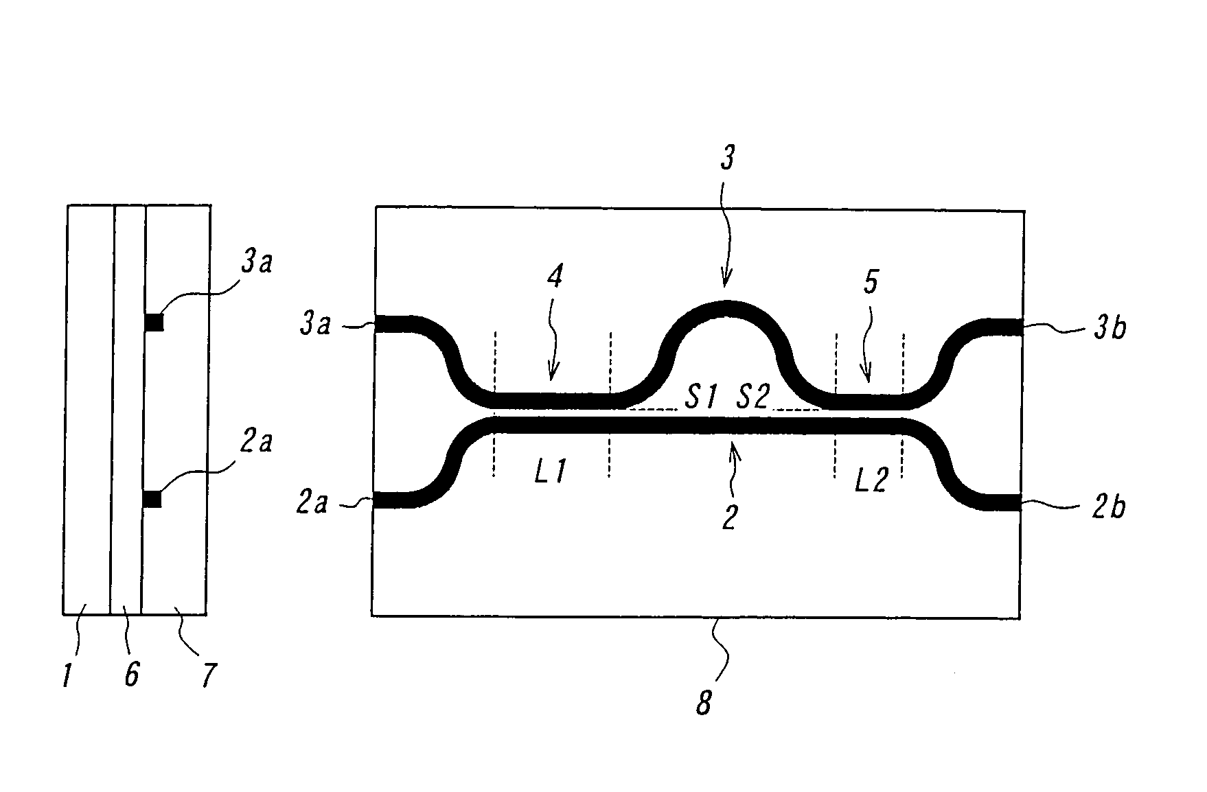
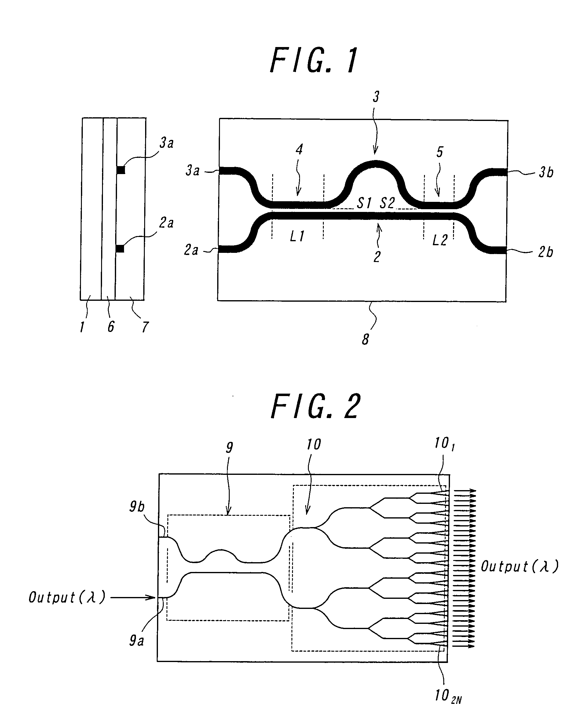
[0065] FIG. 1 shows an optical waveguide coupler circuit device of this invention.

[0066] The polymeric optical waveguide coupler circuit device 8 stable to the changes of ambient temperature comprises two optical waveguide cores 2, 3 formed on the surface of a substrate 1 made of a quartz plate as shown in FIG. 1. The optical waveguide cores 2, 3 are made from a polymer material having a refractive index n.sub.g of 1.508 to 1.568 and a double refraction of 0.008 to 0.01 as shown in the figure, and has a square cross-section with a side of 6 to 8 .mu.m. The material constituting the lower and upper cladding layers 6, 7 covering the optical waveguide cores 2, 3 is a polymer having a refractive index n.sub.c of 1.503 to 1.562 and a double refraction of 0.008 to 0.01.

[0067] The optical waveguide cores 2, 3 form two directional couplers 4, 5 by approaching to and running in parallel with each other at two sites. For the directional coupler 4, the length L.sub.1 of the parallel section is...


PUM


Abstract

The present invention relates to an optical waveguide coupler device. As shown in FIG. 1, the optical waveguide coupler device 8 comprises two optical waveguide cores 2, 3 formed on the surface of a substrate 1. The optical waveguide cores 2, 3 are covered by lower and upper cladding layers 6, 7 both formed on the substrate 1; and the two optical waveguide cores 2, 3 are brought close to and in parallel with each other at two sites to form two directional couplers 4, 5 there. The cross-section and refractive index of each of the optical waveguide cores 2, 3 and the parameters of other elements of the circuit are optimized such that an optical signal is reliably routed by the circuit without undergoing a wavelength shift even when the circuit is exposed to the changes of polarization and ambient temperature.

Description

[0001] 1. Field of the Invention[0002] The present invention relates to a polymer-based optical waveguide circuit stable to the changes of particularly, a polarization and ambient temperature which is profitably used as a wavelength division multiplexer or demultiplexer in, for example, fiber optic communication.[0003] 2. Description of the Related Art[0004] In a dense wavelength division multiplexing (DWDM) system applied to optical carriers belonging to S, C and L bands, the wavelength independent waveguide coupler has been used that is capable of routing optical carriers comprising 80-100 nm bands around 1550 nm into two channels at a specified split ratio, being unaffected with their wavelengths. The coupler that routes optical carriers at a split ratio of 1:1 is called a 3 dB coupler and has been used in multiple fiber optic communication systems.[0005] Such a wavelength independent waveguide coupler includes a Mach-Zehnder interferometer type optical circuit 17 as shown in FIG...

Claims


Application Information

Patent Timeline
Patent Type & Authority Applications(United States)
IPC IPC(8): G02B6/12G02B6/122
CPCG02B6/1221G02B6/12007G02B6/12
Inventor CHEN, BAOXUEISO, MAMORU
Owner NITTA CORP
Why Eureka
Try Eureka