

Semiconductor device
a technology of semiconductor devices and memory cells, applied in semiconductor devices, digital storage, instruments, etc., can solve the problems of increased power consumption in standby state, leakage current in sram memory cells cannot be ignored, and power consumption cannot be increased
- Summary
- Abstract
- Description
- Claims
- Application Information
AI Technical Summary
Benefits of technology
Problems solved by technology
Method used
Image

Examples
embodiment 2
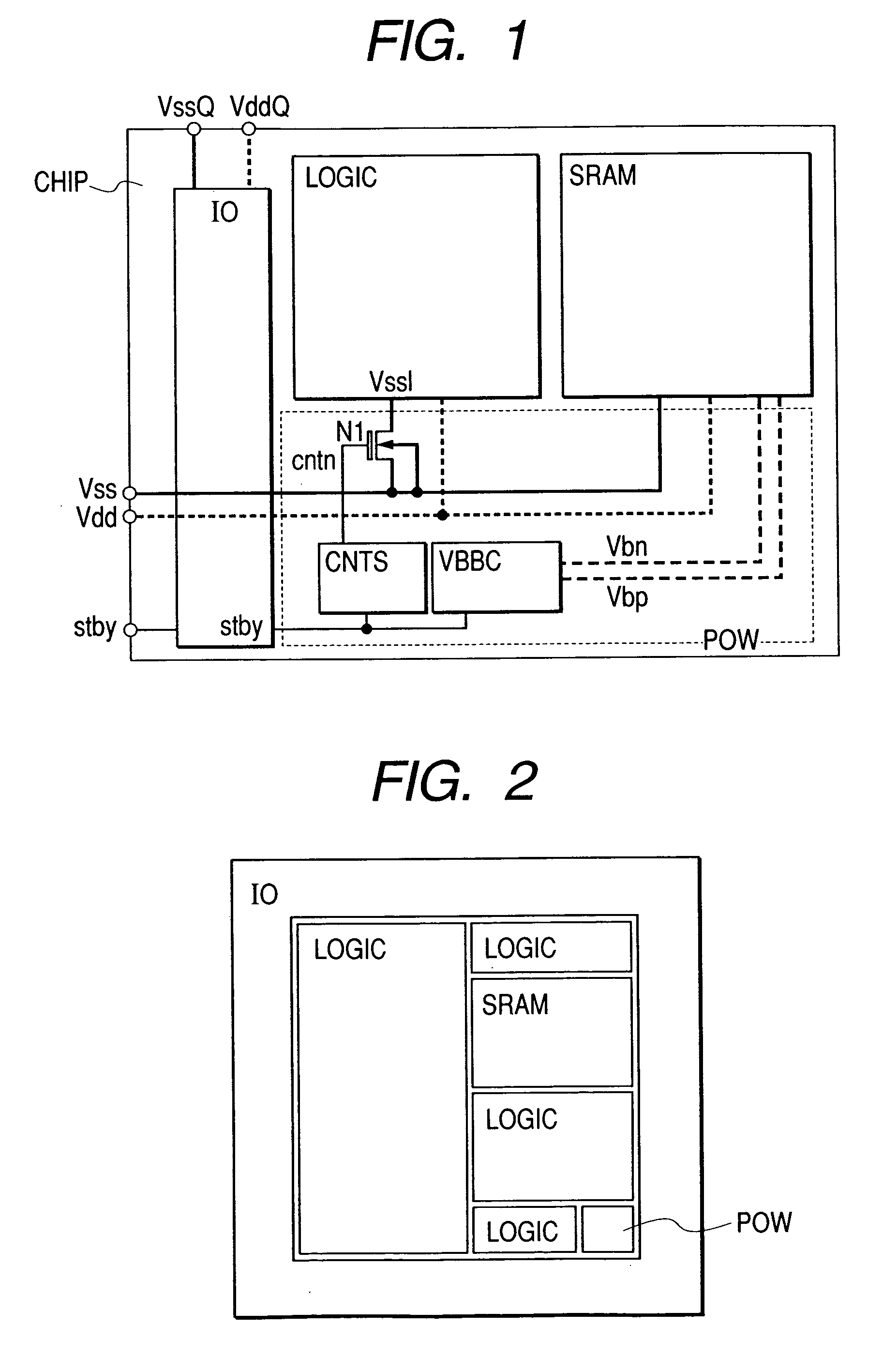
[0062] This embodiment shows a modification of the power switch for use in the logic circuit. FIG. 10 shows a circuit block diagram when the power switch mounted only on the power source Vss of the logic circuit part in the circuit of FIG. 1 is provided in the power sources Vdd and Vss. The two power sources Vdd and Vss of the logic circuit are provided with the switch to cut off the power source. The area is increased by providing the power switch. The leakage current at the time of standby can be cut off more reliably. FIG. 1 illustrates the IO circuit, but is omitted in FIG. 10. The IO circuit in the CHIP is omitted in other drawings.
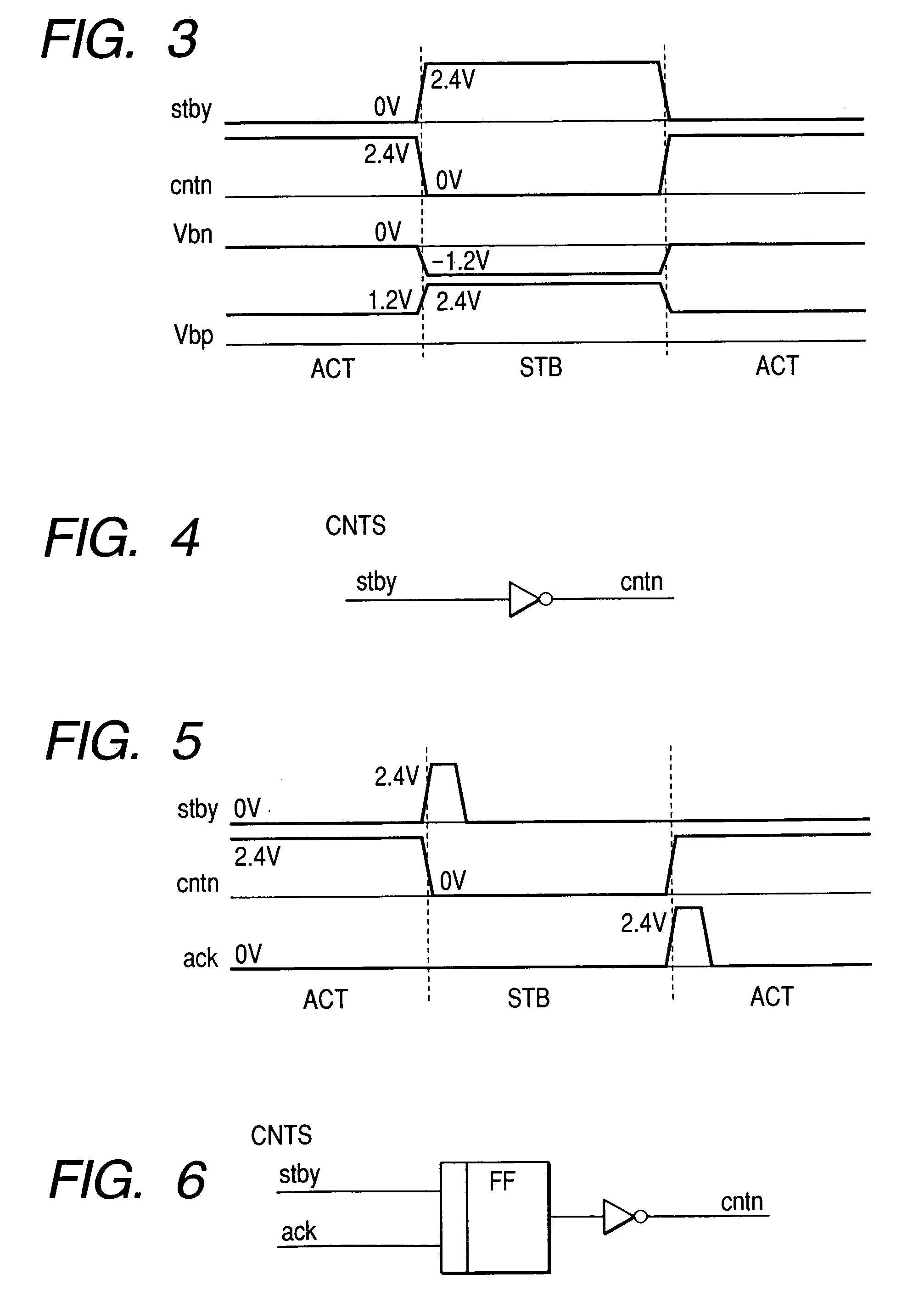
[0063] FIG. 11 shows the voltages of the parts of the circuit when using the circuit of FIG. 10. In this drawing, a signal cntp controlling P1 of the pMOS as a switch for cutting off the Vdd of the logic part is added to the voltages of FIG. 3. The cntp is low in the active state ACT and is high in the standby state STB. The internal circuit of a cir...
embodiment 3
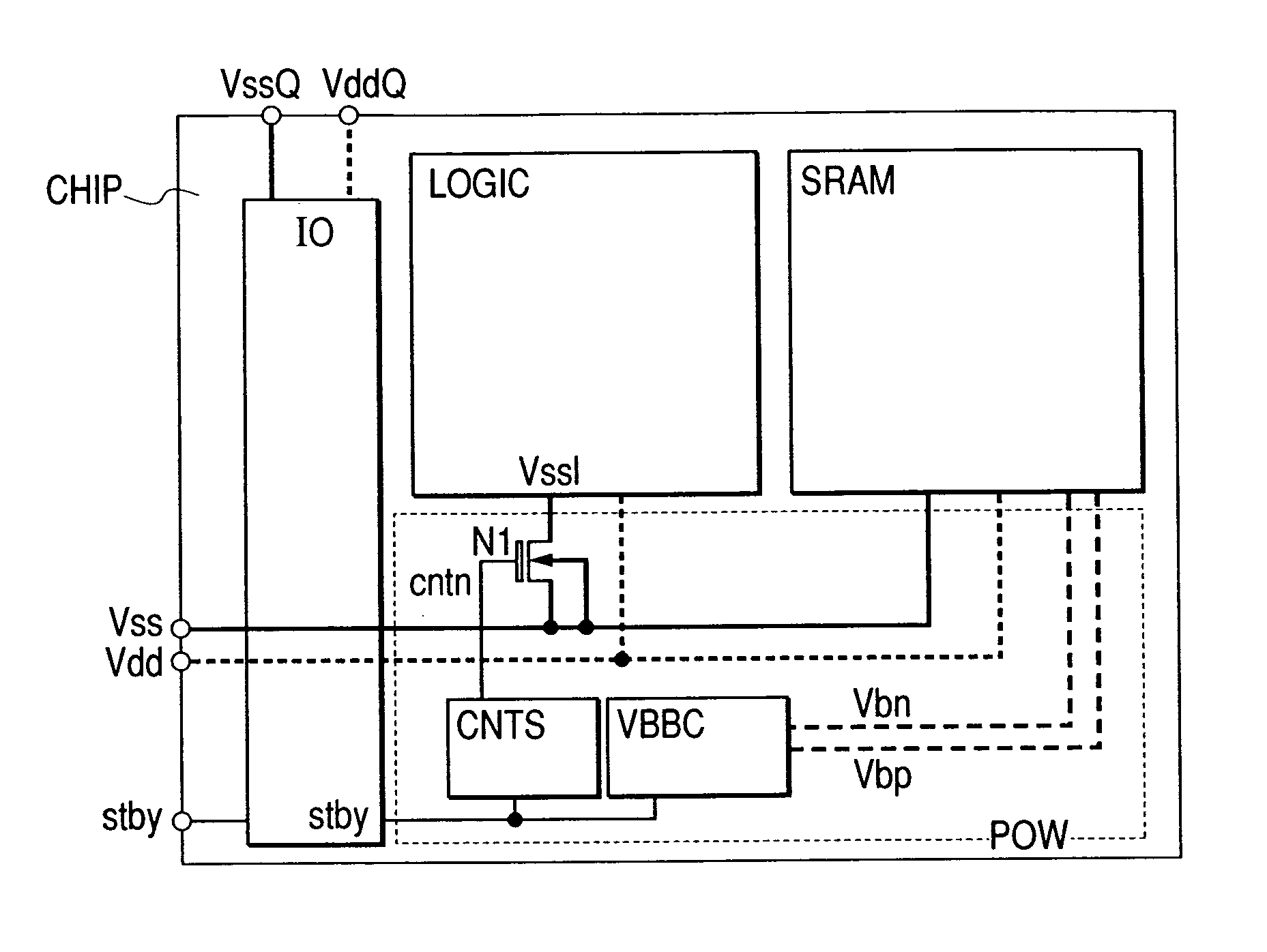
[0069] FIG. 15 schematically shows the entire construction of the LSI consolidating the logic circuit and the SRAM circuit using the present invention. The CHIP as the consolidated LSI includes the logic circuit LOGIC; the static memory circuit SRAM; the nMOS transistor N1 as a switch between the ground voltage line Vss from outside and the ground voltage line Vss1 of the logic circuit; the control circuit CNTS to which the signal stby inputted in the standby state is inputted to be connected to the gate electrode of the N1 outputting the signal cntn controlling the N1; the substrate bias control circuit VBBC controlling the substrate voltages Vbn and Vbp of the SRAM when the stby is inputted; and a circuit CNTV1 controlling the power line Vddm of the SRAM by the stby signal.
[0070] The construction of FIG. 15 is the same as that of the circuit of FIG. 1 except for the CNTV1. Other than the CNTV1, it is operated as in FIG. 1. The CNTV1 is brought into the standby state and the stby s...
embodiment 4
[0073] FIG. 18 shows a modification of the circuit of FIG. 7. In FIG. 7, the power sources of the memory cell array are the Vddma and the Vssma, the power sources of the circuit RWAMP including the circuit driving the bitline are the Vddamp and the Vssamp, and the power sources of other circuits are the Vddper and the Vssper. The power source in the SRAM circuit is divided into three systems. A switch having the N channel type MOS transistor is inserted between the peripheral circuit PERI2 for use in control of the bitline and the power source on the low voltage side. A switch having the P channel type MOS transistor is inserted between the peripheral circuit PERI1 for use in control of the wordline and the power source on the high voltage side. The switches are inserted in the high voltage side and the low voltage side of the three-system power sources to cut off the power sources at the time of standby. In this circuit, the switches constructed by the MOS transistor are inserted i...
PUM
 Abstract
Description
Claims
Application Information