Insulated gate tunnel-injection device having heterojunction and method for manufacturing the same

a technology of heterojunction and tunnel injection, which is applied in the direction of semiconductor devices, diodes, electrical devices, etc., can solve the problems of large channel resistance, difficult reduction of interface states in the interface between silicon oxide film and sic surface, and punching in the channel region

Inactive Publication Date: 2004-04-29
NISSAN MOTOR CO LTD
View PDF5 Cites 129 Cited by
  • Summary
  • Abstract
  • Description
  • Claims
  • Application Information

AI Technical Summary

Problems solved by technology

However, there is a problem in the SiC power MOSFET shown in Japanese Patent Laid-Open-no.
Since the carbon atoms of the carbon cluster are supplied from the oxidizing reaction of the SiC, the generation of the carbon cluster is not avoided, as far as the gate insulation film is formed by the thermally oxidization of the SiC, and the reduction of the interface states in the interface between the silicon oxide film and the SiC surface is difficult.
In light of the above discussion, the carrier mobility in the inversion type channel formed on the top surface of the channel region is very small, and there is a problem in that channel resistance is large.
However, if the channel length is formed too short, as a high voltage is applied to the drain electrode under the condition that the gate and source electrodes are grounded, there is a concern that a punch through occurs in the channel region.
Actually, it is difficult to delineate the channel length to be less

Method used


Image

  • Insulated gate tunnel-injection device having heterojunction and method for manufacturing the same
  • Insulated gate tunnel-injection device having heterojunction and method for manufacturing the same
  • Insulated gate tunnel-injection device having heterojunction and method for manufacturing the same

Examples


first embodiment

1. First Embodiment

[0050] 1.1 Basic Configuration of First Embodiment:

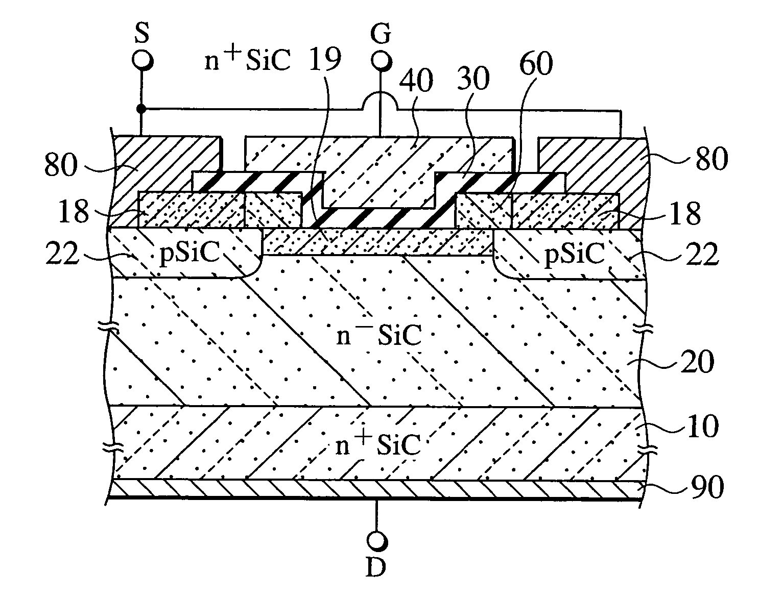
[0051] FIG. 1 shows a basic configuration of a tunnel-injection device associated with a first embodiment of the present invention. FIG. 1 shows cross-sectional views of three adjacent unit cells in the multi-channel structure. In the multi-channel structure, a plurality of gate electrodes 40 and a plurality of source electrodes 80 are mutually arranged in parallel so as to implement an interdigital topology. The gate electrodes 40 and source electrodes 80 are respectively delineated in stripe geometries.

[0052] As shown in FIG. 1, the basic configuration of the tunnel-injection device associated with the first embodiment of the present invention encompasses a reception layer 20 made of a first semiconductor and a plurality of barrier-forming layers 60 made of a second semiconductor having a bandgap-narrower than the first semiconductor. Each of the barrier-forming layer 60 metallurgical contacts with the reception...

second embodiment

2. Second Embodiment

[0088] 2.1 Basic Configuration of Second Embodiment:

[0089] As shown in FIG. 7 a tunnel-injection device associated with a second embodiment of the present invention encompasses a reception layer 20 having a periodic recessed structure at the top surface and a plurality of barrier-forming layers 60, each being in metallurgical contact with the reception layer 20 at the protruding potion of the recessed structure. Similar to the first embodiment, the reception layer 20 is made of a first semiconductor and barrier-forming layer 60 is made of a second semiconductor having a bandgap narrower than the first semiconductor. Here, p.sup.-type lightly doped polysilicon film 60 serves as the barrier-forming layer because the reception layer 20 is made of SiC, for example.

[0090] As shown in FIG. 7, a plurality of gate insulating films 30 are disposed on the barrier-forming layer 60 at the peripheral edge of the gate insulating films, respectively. The gate insulating films 3...

third embodiment

3. Third Embodiment

[0119] 3.1 Basic Configuration of Third Embodiment:

[0120] As shown in FIG. 11, a tunnel-injection device associated with a third embodiment of present invention encompasses a reception layer 20 and a barrier-forming layer 60 buried in the reception layer 20 at the top surface of the reception layer 20. Similar to the first and second embodiments, reception layer 20 is made of a first semiconductor, and the barrier-forming layer 60 is a second semiconductor having a bandgap narrower than the first semiconductor. Each of the buried barrier-forming layer 60 is metallurgical contact with the reception layer 20

[0121] Further as shown in FIG. 11, a plurality of carrier-supplying regions 18 buried in corresponding barrier-forming layers 60 so that each of the carrier-supplying regions 18 can contact with the barrier-forming layer 60, and they supply the carriers to the corresponding barrier-forming layer 60. And a gate insulating film 30 is disposed on the barrier-formin...


PUM


Abstract

The present invention-provides a tunnel-injection device which encompasses, a reception layer made of a first semiconductor, a barrier-forming layer made of a second semiconductor having a bandgap-narrower than the first semiconductor, being in metallurgical contact with the reception layer, a gate insulating film disposed on the barrier-forming layer. The gate electrode controls the width of the barrier generated at the heterojunction interface between the reception layer and the barrier-forming layer so as to change the tunneling probability of carriers through the barrier. The device further encompasses a carrier receiving region being contact with the reception layer and a carrier-supplying region being contact with the barrier-forming layer.

Description

[0001] 1. Field of the Invention[0002] The present invention relates to a switching device using tunnel injection, which are particularly adapted for wide bandgap semiconductor device and a method for manufacturing the switching device. The invention particularly relates to a heterojunction device using an insulated gate structure.[0003] 2. Description of the Related Art[0004] The bandgap of SiC is wide, and it's maximum breakdown field is larger than silicon (Si) one figure. Furthermore, the natural oxide of SiC is silicon oxide (SiO.sub.2), and the thermal oxidation film can be formed easily on the surface of SiC by a method the same as that for Si. For this reason, SiC is anticipated for use in a high-speed / high breakdown voltage switching device used in a battery car, and in-particular when it is used as a high power unipolar / bipolar device, it is hoped that SiC will provide a superior material. For example, Japanese Patent Laid-Open-no. 10-233503 discloses earlier SiC power MOS...

Claims


Application Information

Patent Timeline
IPC IPC(8): H01L21/00H01L21/04H01L29/06H01L29/16H01L29/165H01L29/24H01L29/267H01L29/739H01L29/772H01L29/78H01L29/88H01L31/0328
CPCH01L29/0653H01L29/1602H01L29/1608H01L29/165H01L29/7828H01L29/66068H01L29/772H01L29/7802H01L29/7813H01L29/267H01L29/0878
Inventor KANEKO, SAICHIROUHOSHI, MASAKATSUTHRONGNUMCHAI, KRAISORNHAYASHI, TETSUYATANAKA, HIDEAKIMIHARA, TERUYOSHI
Owner NISSAN MOTOR CO LTD
Why Eureka
Try Eureka