MEMS planar antenna array

a planar antenna array and antenna technology, applied in the direction of antennas, antenna feed intermediates, antenna details, etc., can solve the problems of affecting the performance of each antenna, and difficulty in housing a corresponding plurality of microstrip antennas, etc., to achieve the effect of convenient manufactur

Inactive Publication Date: 2004-04-29
HANEI
View PDF5 Cites 33 Cited by
  • Summary
  • Abstract
  • Description
  • Claims
  • Application Information

AI Technical Summary

Benefits of technology

0019] The present invention provides a microstrip, or printed circuitboard antenna that is made with MEMSs to vary the actual physical length of the printed line active element radiators. The MEMSs can be used to form selectable connected conductive sections that vary the length, position, and shape of the antenna active element. In this manner, the antenna operating frequency, bandpass, or beam pattern can be modified. In addition, the active element is situated in a lattice of MEMS parasitic elements. The MEMS devices

Problems solved by technology

As a result, the designers must increase the performance of components or device subsystems while reducing their size, or placing these components in less desirable locations.
However, a wireless device that is expected to operate at a plurality of different frequencies may have difficulty housing a corresponding plurality of microstrip antennas.
Even if all the microstrip antennas could be housed, the close proximity of the several microstrip antennas may degrade the performance of each antenna.
Mechanical manipulation generally requires additional parts that take up room and degrade reliability.
As a

Method used


Image

  • MEMS planar antenna array
  • MEMS planar antenna array
  • MEMS planar antenna array

Examples


Embodiment Construction

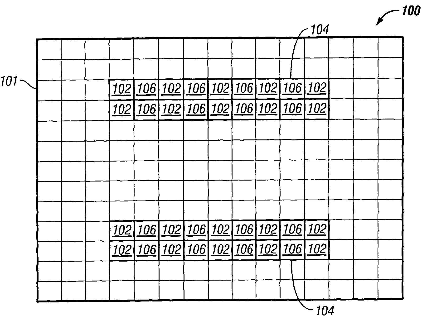
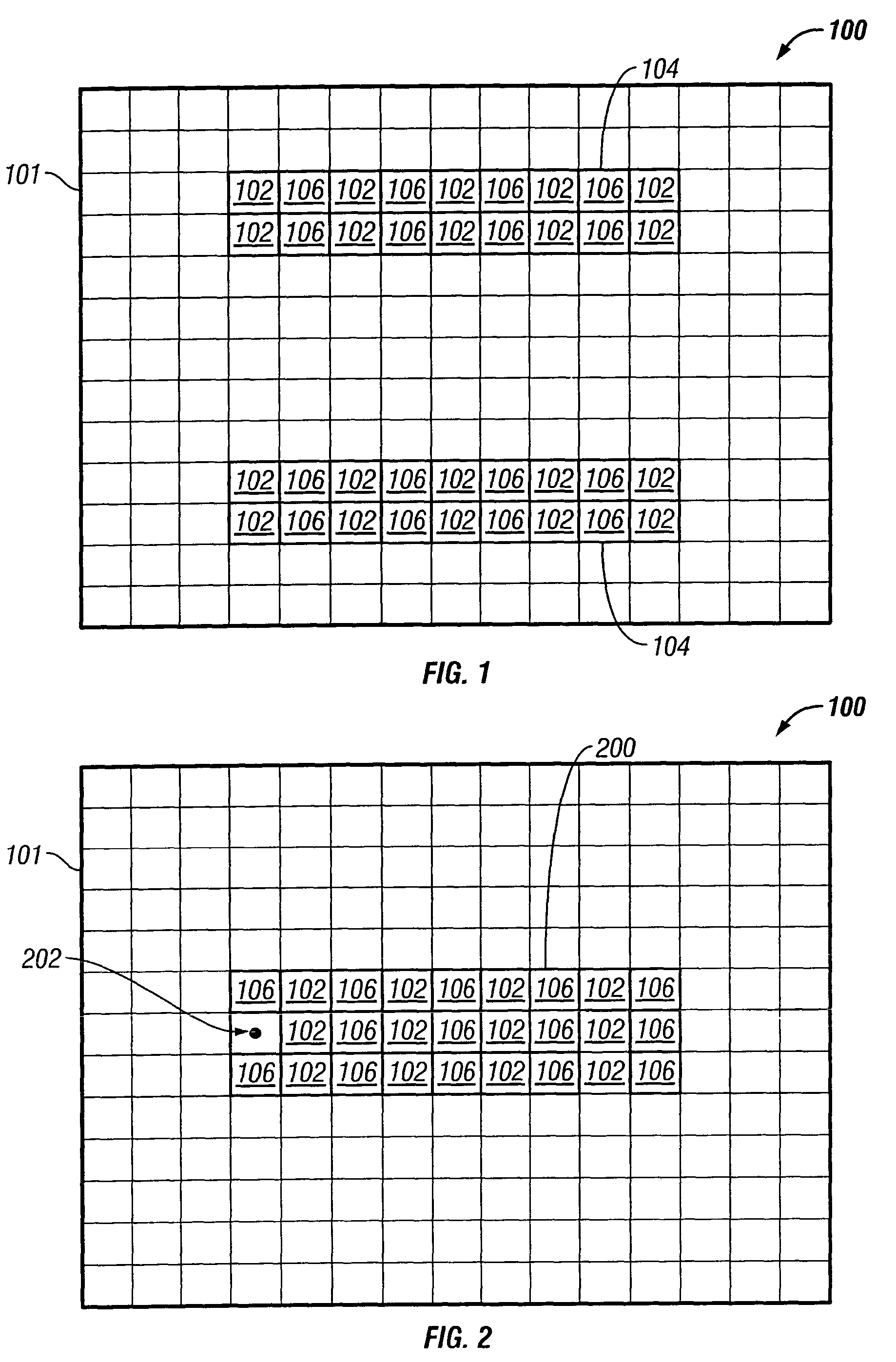
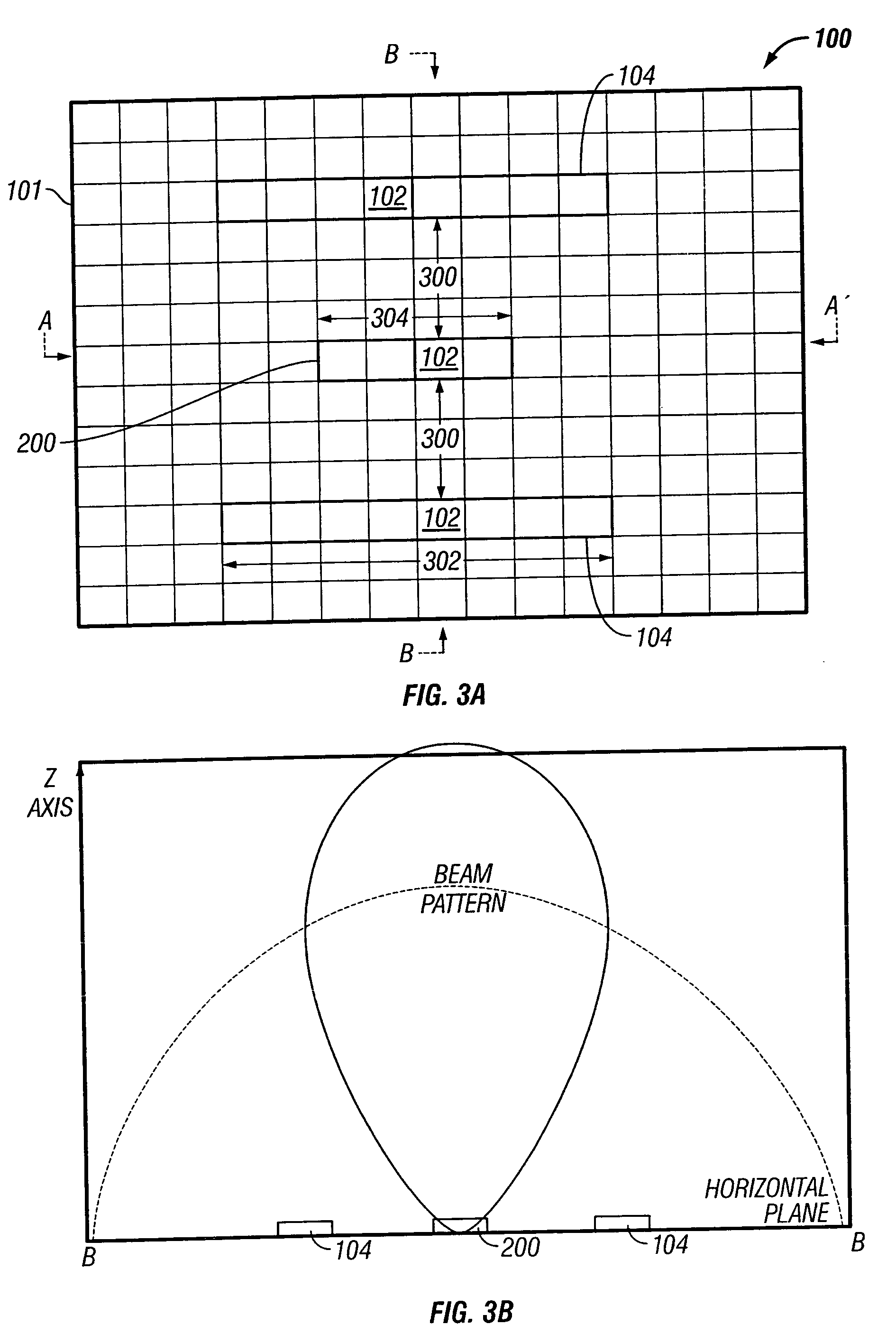
[0051] FIG. 1 is a plan view of the present invention microelectromechanical switch (MEMS) planar antenna array. The antenna array 100 comprising a planar field 101 of MEMSs 102. A lattice of parasitic elements can be formed by selectively connecting a MEMS 102 in the field 101. As shown, a lattice is formed with two parasitic elements 104. Each parasitic element 104 includes ten MEMS sections 102. Although a rectangular field 101 is shown, the present invention is not limited to any particular field shape. As explained in more detail below, the field 101 may be comprised of MEMS 102 exclusively, or a combination of MEMS 102 sections and non-switching (non-MEMS) conductive areas. In other aspects of the array 100, the field may include non-switching non-conductive areas in combination with MEMS 102, or further in combination with MEMS 102 and non-switching conductive areas.

[0052] In one aspects of the antenna array 100, the field can be comprised exclusively of connected MEMS sectio...


PUM


Abstract

A MEMS planar antenna array is provided comprising a planar field of MEMSs. A lattice of parasitic elements can be formed by selectively connecting at least one MEMS in the field. An antenna active element is formed by selectively connecting MEMS in the field. Alternately, both the parasitic elements and the active elements are formed by connecting MEMS. The parasitic elements have a number, shape, length, distance from the active element, and position with respect to the active element that are formed in response to selectively connecting MEMS in the field. Further, a plurality of different parasitic element lattices can be formed in response to selectively connecting MEMS in the field. Likewise, the active element has a length, shape, and position that is formed in response to selectively connecting MEMS. Patch, monopole, and dipole antennas are among the antenna types that can be formed from the MEMS.

Description

BACKGROUND OF THE INVENTION[0001] 1. Field of the Invention[0002] This invention generally relates to wireless communications antennas and, more particularly, to a selectable antenna array formed from a planar field of microelectromechanical switches (MEMSs).[0003] 2. Description of the Related Art[0004] The size of portable wireless communications devices, such as telephones, continues to shrink, even as more functionality is added. As a result, the designers must increase the performance of components or device subsystems while reducing their size, or placing these components in less desirable locations. One such critical component is the wireless communications antenna. This antenna may be connected to a telephone transceiver, for example, or a global positioning system (GPS) receiver.[0005] Wireless telephones can operate in a number of different frequency bands. In the US, the cellular band (AMPS), at around 850 megahertz (MHz), and the PCS (Personal Communication System) band,...

Claims


Application Information

Patent Timeline
IPC IPC(8): H01Q3/24
CPCH01Q3/24
Inventor TRAN, ALLEN
Owner HANEI
Why Eureka
Try Eureka