Method to form alpha phase Ta and its application to IC manufacturing

a technology of alpha phase ta and ic manufacturing, which is applied in the direction of ion implantation coating, coating, electrical equipment, etc., can solve the problems of significant drop, oxidation and corrosion resistance, and serious thermal stress induced by voids

Inactive Publication Date: 2004-07-08
CHARTERED SEMICONDUCTOR MANUFACTURING
View PDF15 Cites 38 Cited by
  • Summary
  • Abstract
  • Description
  • Claims
  • Application Information

AI Technical Summary

Problems solved by technology

Nonetheless, copper is a fast migrating species in silicon based devices, and its inherent chemical reactivity renders it susceptible to oxidation and corrosion.
For instance, some of these advantages may be mutually contradictory, in that they cannot be simultaneously present in a single embodiment.
When a

Method used


Image

  • Method to form alpha phase Ta and its application to IC manufacturing
  • Method to form alpha phase Ta and its application to IC manufacturing
  • Method to form alpha phase Ta and its application to IC manufacturing

Examples


Embodiment Construction

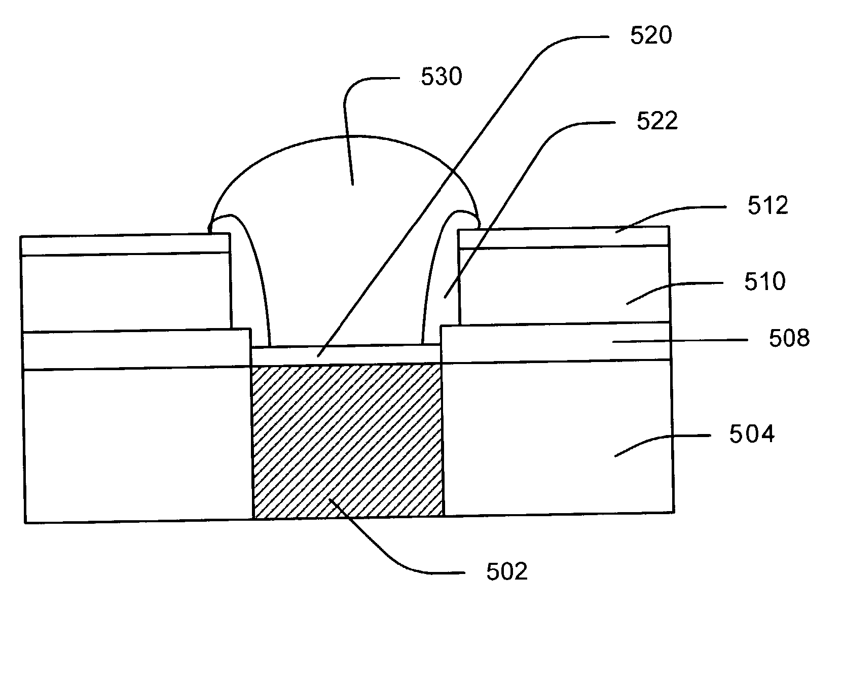
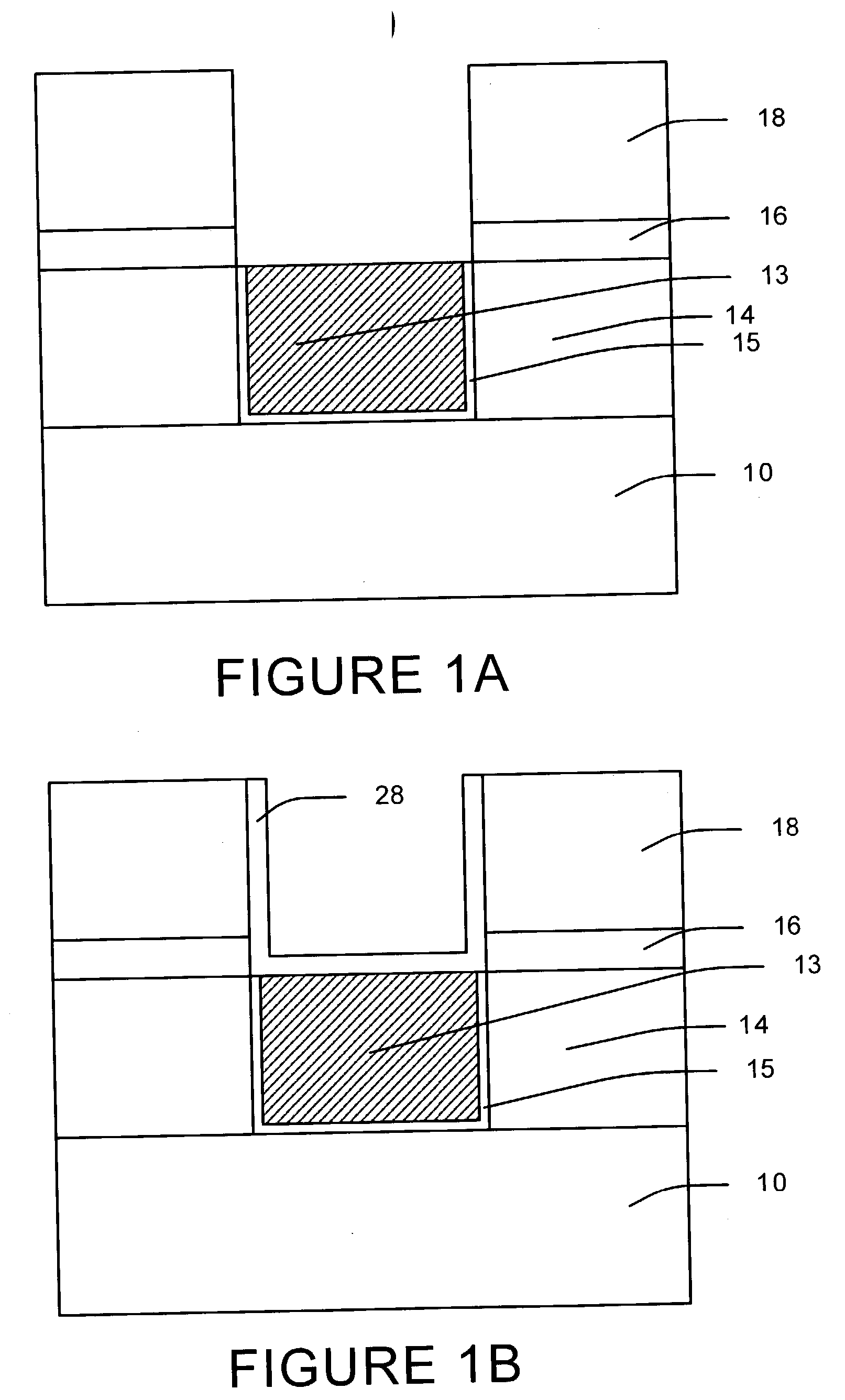
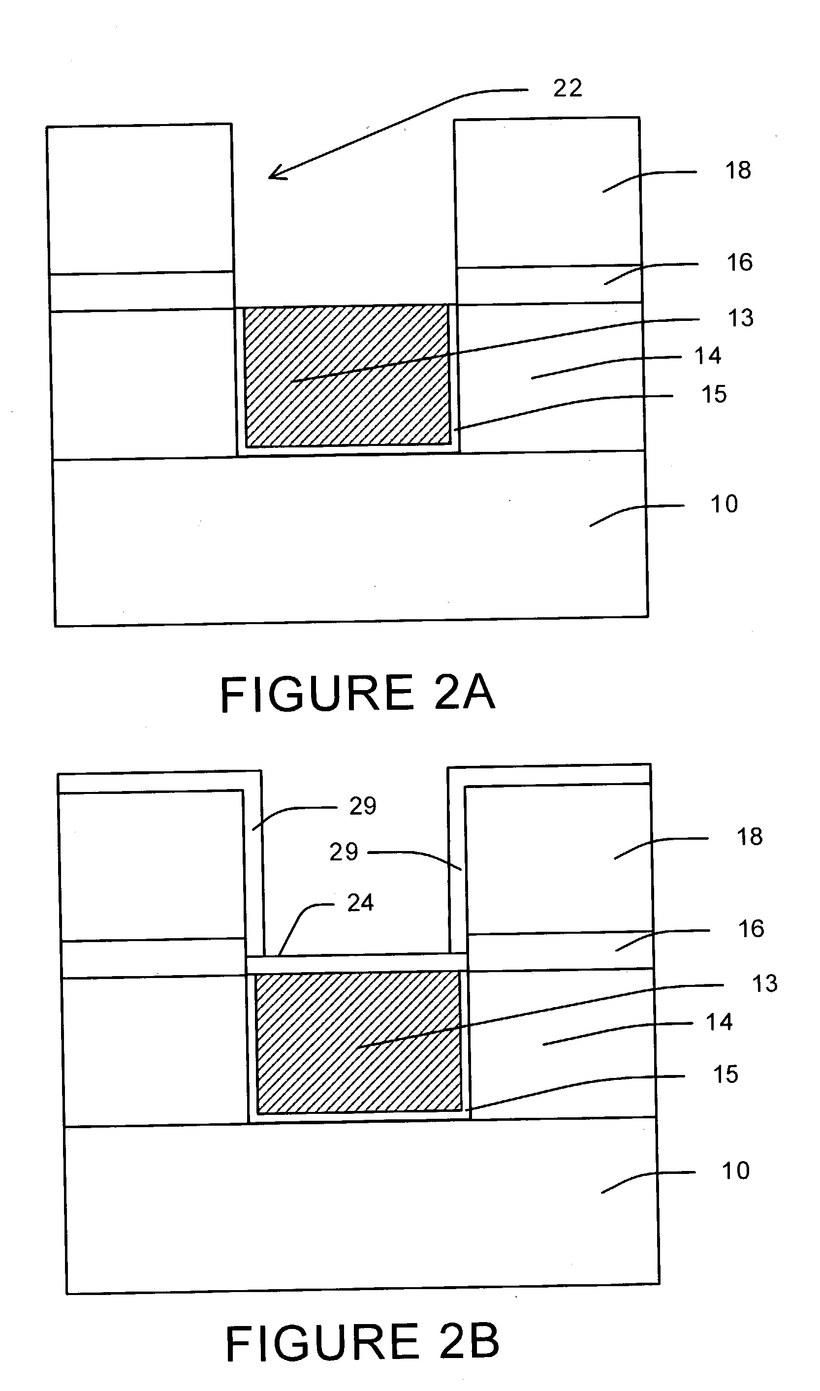
[0096] FIGS. 2A thru 2C show a structure formed by preferred embodiments of the invention.

[0097] As shown in FIG. 2A, a substrate 10 is provided. A first dielectric layer 14 such as oxide layer is formed over the substrate.

[0098] A hole / trench in the dielectric layer is formed by single or dual damascene methods.

[0099] A copper layer 13 (e.g., Metal feature) is formed filling the opening. The copper layer can be formed by a deposition and chemical-mechanical polish (CMP) (e.g., Damascene process).

[0100] A barrier layer (or etch stop layer) 16 is formed over the dielectric layer 14 and the copper layer 13. The buffer layer can be comprised of oxide, nitride, or carbide.

[0101] A second dielectric layer 18 is formed over the copper layer 13 and the barrier layer 16.

[0102] Still referring to FIG. 2A, an opening 22 in the second dielectric layer 18 and the barrier layer 16 is formed to expose the copper layer.

[0103] A barrier layer (24 29) is formed on the copper layer 13 and sidewalls i...


PUM

PropertyMeasurementUnit
Lengthaaaaaaaaaa
Lengthaaaaaaaaaa
Lengthaaaaaaaaaa

Abstract

A method of sputtering a Ta layer comprised of alpha phase Ta on a Cu layer. An embodiment includes a Ta sputter deposition on a Cu surface at a substrate temperature less than 200° C. Another embodiment has a pre-cooling step at a temperature less than 100° C. prior to Ta layer sputter deposition. In another non-limiting example embodiment, a pre-clean step comprising an inert gas sputter is performed prior to the tantalum sputter. Another non-limiting example embodiment provides a semiconductor structure comprising: a semiconductor structure; a copper layer over the semiconductor structure; a tantalum layer on the copper layer; the tantalum layer comprised alpha phase Ta; a metal layer on the tantalum layer.

Description

BACKGROUND OF INVENTION[0001] 1) Field of the Invention[0002] This invention relates generally to fabrication of semiconductor devices, and to the fabrication of metal layers comprised of alpha phase Tantalum (Ta) and more particularly to Ta layers comprised of alpha and beta phase tantalum.[0003] 2) Description of the Prior Art[0004] As ultra-large scale integrated (ULSI) devices extend into deep submicron generations, new interconnect schemes and materials are essential to drive performance and reliability. Owing to its lower bulk electrical resistivity (1.7-2.2 micro-ohm-cm) and higher electromigration resistance, copper has begun to displace aluminum as the interconnect material of choice. Nonetheless, copper is a fast migrating species in silicon based devices, and its inherent chemical reactivity renders it susceptible to oxidation and corrosion. Hence, encapsulation of the copper is essential, and a conductive barrier should be a suitable encapsulant that can act both as an e...

Claims


Application Information

Patent Timeline
IPC IPC(8): C23C14/16C23C14/54H01L21/285H01L21/60H01L21/768
CPCC23C14/165Y10T428/12903H01L21/2855H01L21/76843H01L21/76846H01L24/03H01L24/05H01L24/11H01L24/12H01L2224/0401H01L2224/13022H01L2224/13099H01L2924/01005H01L2924/01006H01L2924/01013H01L2924/01014H01L2924/01018H01L2924/01022H01L2924/01029H01L2924/0105H01L2924/01073H01L2924/01082H01L2924/014H01L2924/04953H01L2924/05042H01L2924/01019H01L2924/01023H01L2924/01024H01L2924/01033H01L2224/05001H01L2224/0554Y10T428/12674Y10T428/12819C23C14/541H01L2924/351H01L2924/00
Inventor SEET, CHIM SENGZHANG, BEI CHAOLIEW, SAN LEONGSUDIJONO, JOHNCLARE YONG, LAI LIN
Owner CHARTERED SEMICONDUCTOR MANUFACTURING
Why Eureka
Try Eureka