Method and mold for fabricating article having fine surface structure

a surface structure and fine technology, applied in the field of fine structure fabrication on the surface, can solve the problems of poor mass-productivity, expensive apparatus, and inability to be put into practical us

Inactive Publication Date: 2004-07-15
RICOH OPT IND CO LTD
View PDF3 Cites 50 Cited by
  • Summary
  • Abstract
  • Description
  • Claims
  • Application Information

AI Technical Summary

Problems solved by technology

Method (B) requires an apparatus capable of high precision control, therefore, the apparatus is costly.
Because of poor mass-productivity and reproducibility of method (B), it has not been put into practical use.
However, there exists a difficulty in fabricating a fine surface structure on an object material by using dry etching as in method (D).
But fabrication of a high surface structure is difficult because a large amount of the object material has to be etched.
As a result, processing time (here, the etching time) becomes long, and fabrication precision degrades exponentially with the etching tim

Method used


Image

  • Method and mold for fabricating article having fine surface structure
  • Method and mold for fabricating article having fine surface structure
  • Method and mold for fabricating article having fine surface structure

Examples


second example

[0133] An optical element used in optical communication, for example, for coupling two fibers, was fabricated by a method shown in the second example.

[0134] The optical element includes a number of lenses each having a diameter of 50 .mu.m made of synthetic silica. The curvature radius of each lens was 6.16 .mu.m, and the height of each lens was 28.0 .mu.m.

[0135] This optical element was fabricated following the procedure below.

[0136] (1) It was decided to fabricate a silicon mold by transferring an object surface shape onto a silicon substrate, and the surface shape of the mold had a height equal to the object height 28.0 .mu.m multiplied by a factor of (15.5 / 28.0), in other words, to fabricate a mold scaled down by 0.55 relative to the object surface shape, that is, n=1.82. When transferring the object surface shape from a resist onto the silicon substrate, the selection ratio was set to be 1.0.

[0137] (2) After transferring the surface shape from the resist to the silicon substrat...

third example

[0179] Below, a third example of a method of fabricating an optical element the same as that illustrated in FIGS. 4A through 4D, and FIGS. 5A through 5D is described below. This optical element, for example, is used for coupling two fibers. In this example, a detailed configuration of the optical element is introduced, and it is represented by a reference number 100.

[0180] FIGS. 6A and 6B are a plan view and a cross-sectional view, respectively, showing a configuration of the optical element 100, where the cross-sectional view in FIG. 6B is obtained along the X-X line in FIG. 6A.

[0181] As shown in FIGS. 6A and 6B, the optical element 100 includes a large number of lenses 102 formed on two sides of a synthetic silica substrate 110. The lenses 102 are arranged in a matrix manner on each side of the silica substrate 110. Each of the lenses 102 is 0.784 mm in diameter (.PHI..sub.0), and 40 .mu.m in height (H.sub.0).

[0182] As shown in FIG. 6A, the lenses 102 on the two sides of the silic...

fourth example

[0263] A fourth example of a method of fabricating an optical element the same as that illustrated in FIGS. 6A and 6B, or in FIGS. 7A and 7B is described below. The optical element for this example is used for coupling two fibers.

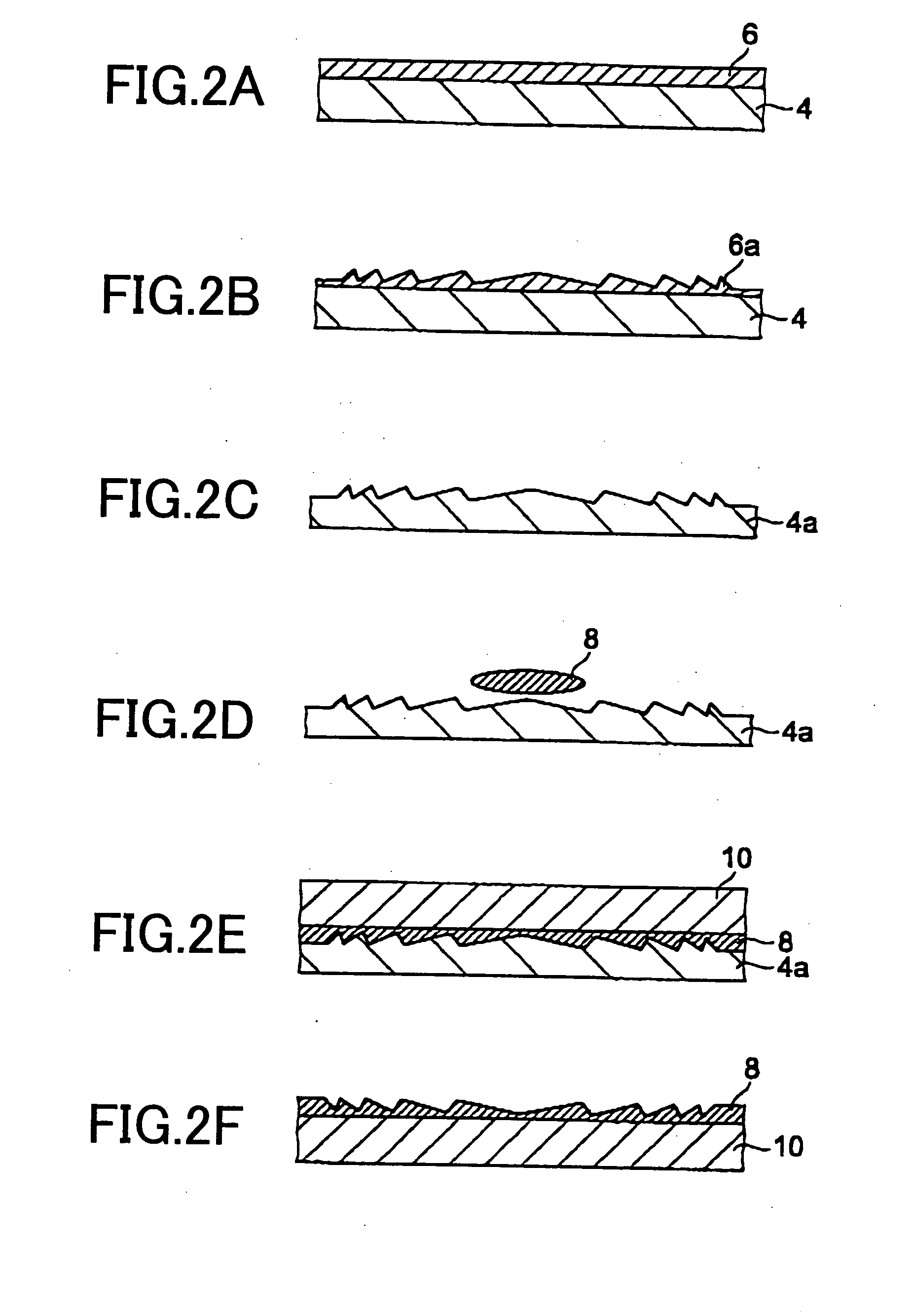
[0264] In this example, a preliminary surface structure was fabricated following the steps shown in FIGS. 13A and 13B.

[0265] FIGS. 13A and 13B are cross-sectional views showing the steps of forming a preliminary surface structure of the optical element 100 using a method of the fourth example.

[0266] First, a mask used in lithography for shielding the lenses 102 was prepared. The diameter of each shielding portion of the mask was essentially the same as the object diameter of each of the lenses 102.

[0267] In the step shown in FIG. 13A, on a silica substrate 210, a photo-conducting material 214 was applied uniformly to a thickness of 5 .mu.m by using a spinning coater. The photo-conducting material 214 used here was the product OFPR-5000-500 of Tokyo Ohka Kog...


PUM

PropertyMeasurementUnit
Timeaaaaaaaaaa
Thicknessaaaaaaaaaa
Shrinkageaaaaaaaaaa

Abstract

A method of fabricating a mold and a method of fabricating an article with the mold is disclosed that is capable of fabricating a high three-dimensional surface structure and extending the service life of the mold. A mold having a fine surface shape of a height less than an object height is fabricated, then the fine surface shape of the mold is transferred to an intermediate mold by dry-etching, and then the fine surface shape of the intermediate mold is further transferred to a final article material by dry-etching. In each transfer step by dry-etching, the etching selection ratio is appropriately adjusted to increase the height of the fine surface structure step by step, so that the fine surface shape of the final article material has the object height. On the surface of the final article material, a preliminary pattern of the object surface shape may be formed beforehand to reduce the required thickness of the curable resin.

Description

[0001] 1. Field of the Invention[0002] The present invention relates to a method of fabricating a fine structure on a surface of an article to produce new optical, mechanical, or physical properties of the article. This method of fabricating a fine structure is applicable to fabrication of, for example, a MLA (micro-lens array), a diffractive optical element, a deflecting optical element, a refractive optical element, a complex refractive optical element, a fiber-related optical element, a beam splitter, and so on. Particularly, this method of fine structure fabrication is suitable for fabrication of an optical element having a dimension less than about 10 mm. Furthermore, this method is applicable to a surface treatment for a micro-machine, mechanically swingable parts of an automobile engine, a compressor of an air conditioner, and articles in various other fields.[0003] 2. Description of the Related Art[0004] In the related art, quite a few techniques have been proposed for fabri...

Claims


Application Information

Patent Timeline
IPC IPC(8): B29C33/38B29C35/08B29C37/00B29D11/00
CPCB29C33/3842B29C35/0894B29D11/00365B29C2035/0827B29D11/00278B29C37/0053B29C35/08
Inventor UMEKI, KAZUHIRO
Owner RICOH OPT IND CO LTD
Why Eureka
Try Eureka