The proximity method can be free from such problems, but, if the clearance between the mask and the workpiece becomes smaller than the largest size of
dust particles, similar damage of the mask may occur.
Therefore, it is difficult to improve the resolution by decreasing the proportional constant.
Even where an
excimer laser is used, it is difficult for a projection exposure apparatus to form a pattern not greater than 0.10 .mu.m.
Additionally, if there is any
light source having shorter
wavelength present,
optical materials to be used for the projection optical
system (i.e. lens glass materials) could not transmit exposure light of such shorter
wavelength, and thus (because of
resultant failure of projection upon a workpiece to be exposed) the exposure would end in failure.
For these reasons, it is very difficult to develop a practical
glass material having a sufficiently large transmissivity to exposure light of a
wavelength not greater than 150 nm, corresponding to a fine pattern of 0.10 .mu.m or narrower.
These factors also make the development of a practical
glass material difficult.
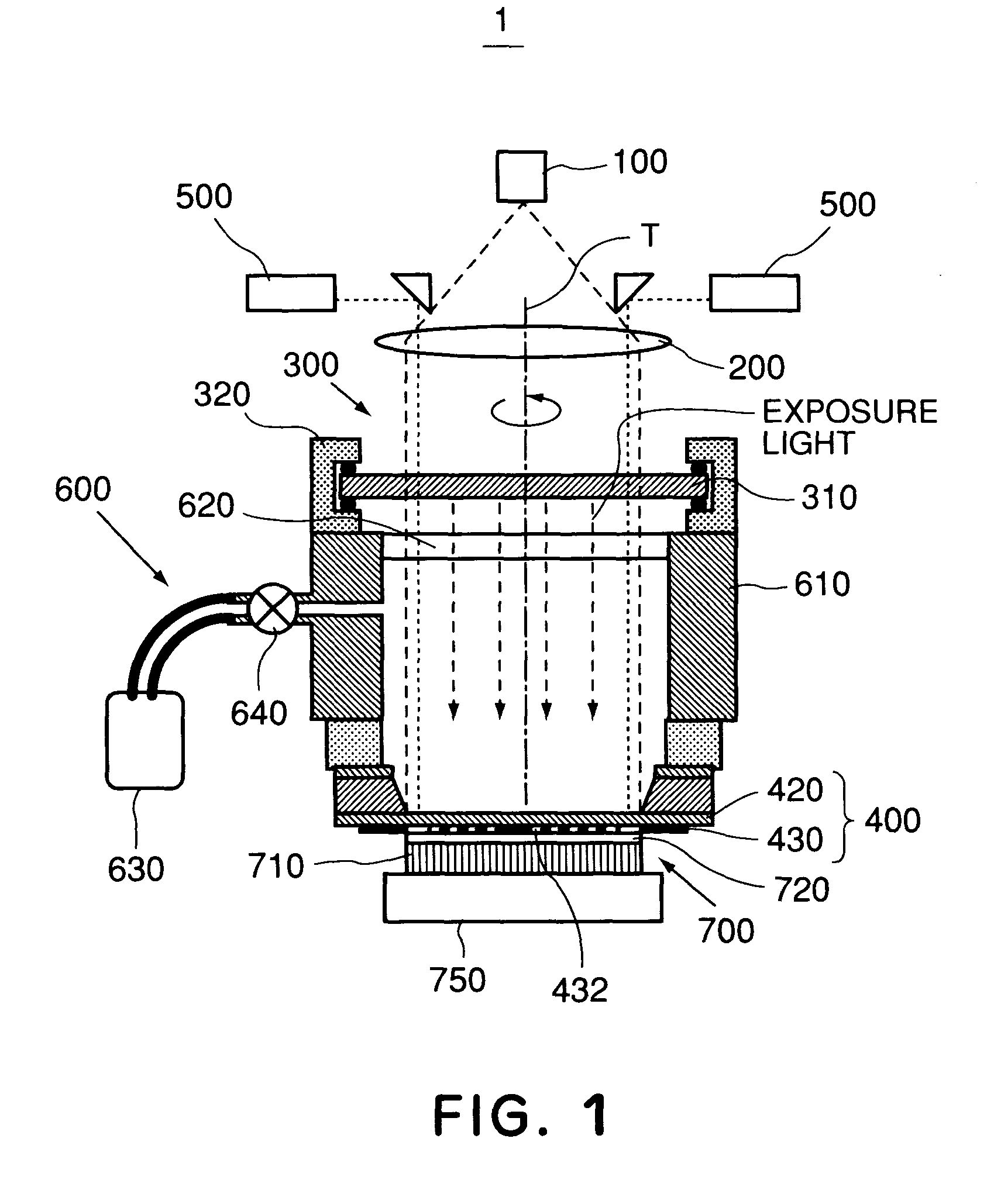
Actually, however, to keep the clearance between the mask surface and the
resist surface to be not greater than 100 nm throughout the whole mask surface is difficult to accomplish, because of the limit of the surface precision of the mask or the substrate and due to tilt or the like involved in the positional alignment between the mask and the substrate.
Any irregularity in clearance between the mask and the substrate may cause non-uniformness of exposure pattern or local crush of the
resist by the mask.
Thus, in a lithographic exposure process using near-field light, there is a possibility that, if the exposure is carried out without controlling the polarization of exposure light, the intensity of near-field light leaking from the small openings formed in a mask changes in dependence upon the direction of polarization of exposure light with respect to the lengthwise direction of the small opening, thereby to cause non-uniformness in exposure pattern.
Therefore, as compared with a mask without such
polarizer, the productivity is low and the cost is high.
The cost of the mask may cause an increase in the cost of semiconductor products.
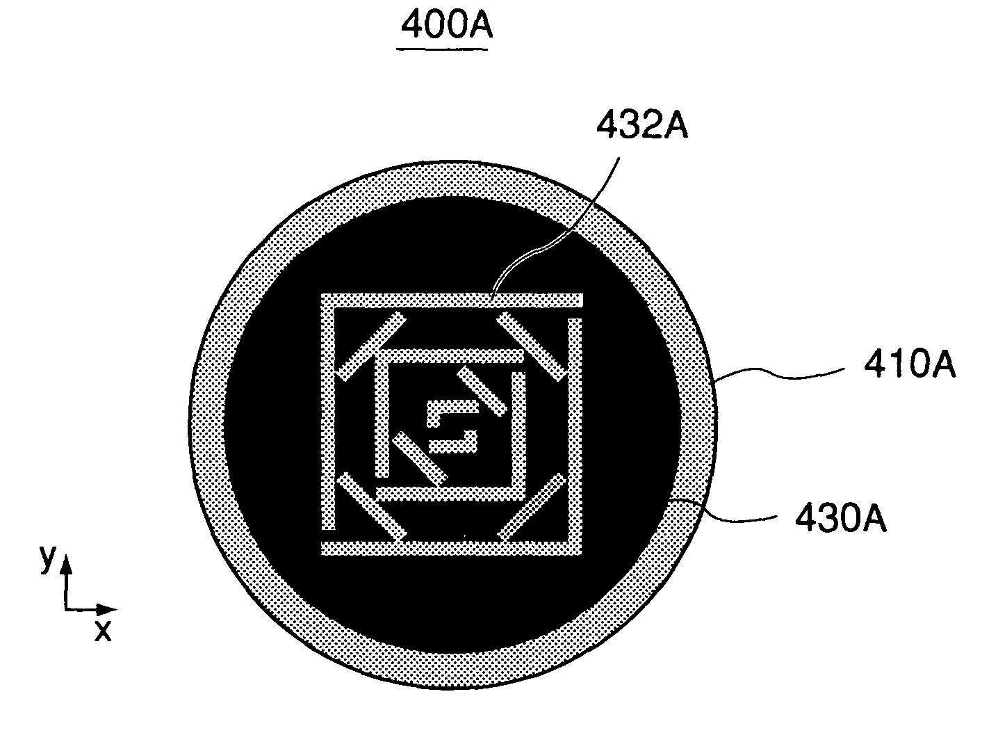
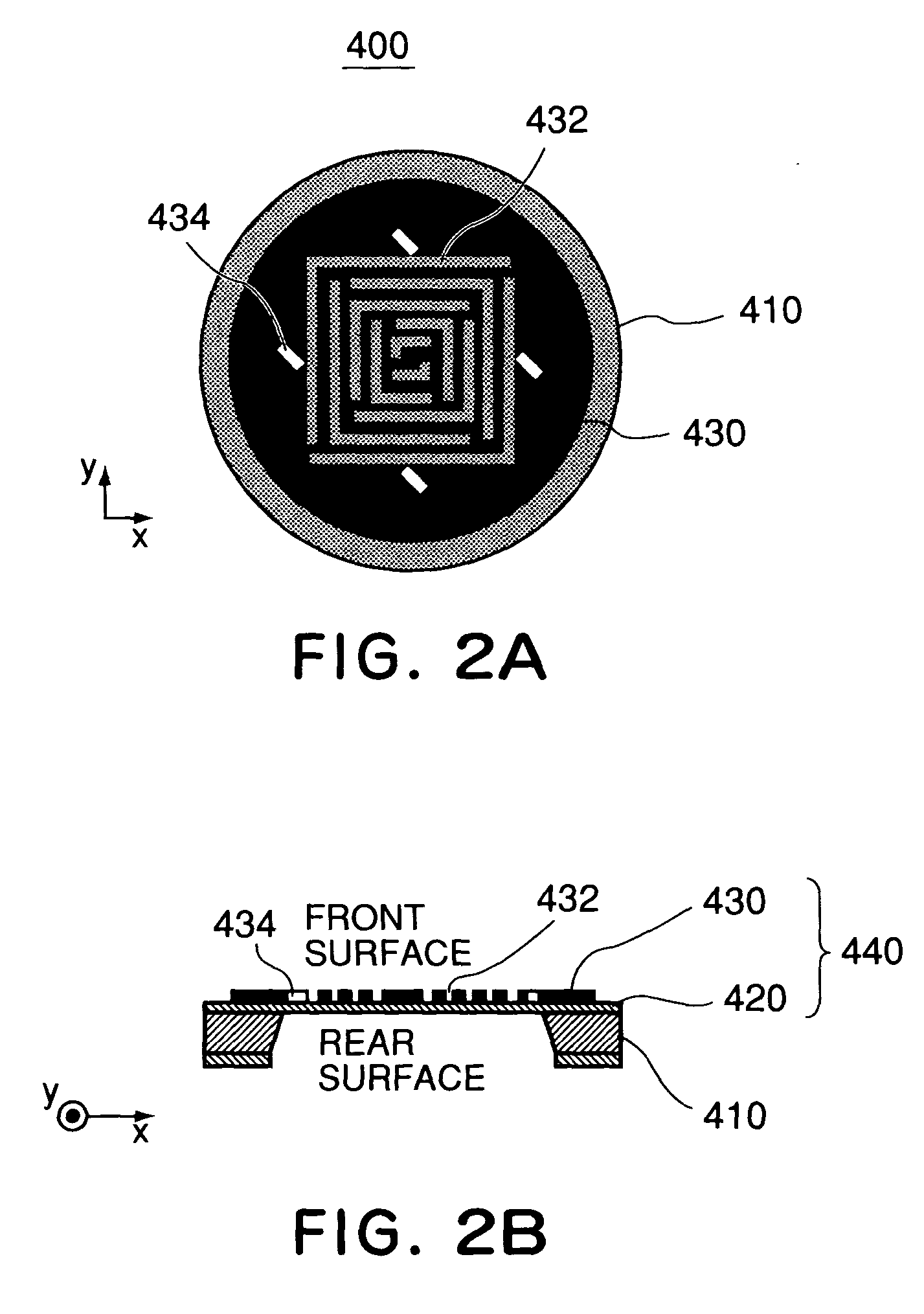
However, if the light blocking film 430 is too thin, it may cause leakage of light from a portion other than the small openings 432.
If the surface of the light blocking film 430 at a side to be contacted to the
resist 720 is not flat, the film can not be well closely contacted to the resist 720 and it may cause non-uniform exposure.
If the width of the patterns of the small opening 432 is larger than 100 nm, not only the near-field light but also direct light having strong
light intensity can transmit the mask 400, with an undesirable result that the light quantity level changes largely with th pattern.
Also, if the width is less than 1 nm, the exposure itself is not unattainable, but the intensity of near-field light escaping from the mask 400 becomes very small so that, impractically, it takes a long time to complete the exposure.
Thus, if the size of the small openings is uneven, the degree of exposure of the resist 720 becomes uneven which makes it difficult to accomplish uniform
pattern formation.
In the non-closely-contacted portions, the small openings and the plate 700 are disposed out of the range in which the near-field light functions, such that non-uniform exposure would result.

