
Integrated optical spectrometer with high spectral resolution in particular for high-speed telecommunications and metrology and a method for manufactruing same

a technology high spectral resolution, which is applied in the field of integrated optical spectrometer with high spectral resolution, can solve the problems of limiting the transmission range, limiting the wavelength routing capacity, and all of the known devices are expensiv

Inactive Publication Date: 2004-07-22
COMMISSARIAT A LENERGIE ATOMIQUE ET AUX ENERGIES ALTERNATIVES
View PDF11 Cites 19 Cited by
  • Summary
  • Abstract
  • Description
  • Claims
  • Application Information

AI Technical Summary

Problems solved by technology

This process is limited by the wavelength routing capacities, by the available power for the amplifiers and by the non-linear effects such as the stimulated Raman effect, the stimulated Brillouin effect and above all, the four-wave mixing that constitutes a limit for wavelength separation.
The growth of requirements in terms of transmission capacity makes development of an inter-channel spacing of 0.4 nm (50 GHz) probable, although the non-linear effects currently limit the transmission range.
All of these known devices are expensive, require large amounts of space and are fragile.
Moreover, their working frequencies are approximately equal or less than 100 Hz and they do not make it possible to assure a resolving power of greater than 30,000 over more than 40 nm.
Furthermore, certain known multiplexers / demultiplexers could be utilized as optical spectrum analyzers but these devices do not make it possible to perform measurements of optical spectra and execute only those multiplexing functions compatible with the standard ITU 50 GHz.
Moreover, these known devices do not make it possible to directly determine the Bragg wavelengths having a sufficiently elevated precision.

Method used


Image

  • Integrated optical spectrometer with high spectral resolution in particular for high-speed telecommunications and metrology and a method for manufactruing same
  • Integrated optical spectrometer with high spectral resolution in particular for high-speed telecommunications and metrology and a method for manufactruing same
  • Integrated optical spectrometer with high spectral resolution in particular for high-speed telecommunications and metrology and a method for manufactruing same

Examples


Embodiment Construction

[0107] An object of the present invention is the realization of a compact, cost-optimized spectrometer that makes it possible to cover the useful spectrum for the third telecommunications window (conventional band or C-band, and long band or L-band). The spectral band to be covered in order to satisfy the current telecommunications market is of the order of 120 nm. Furthermore, the current ITU grid is 50 GHz, which corresponds to a separation of about 0.4 nm between channels (the number of channels being equal to 300).

[0108] An essential area of application of this high-resolution and wide range spectrometer is that of very high spectral density telecommunications (utilizing the DWDM method).

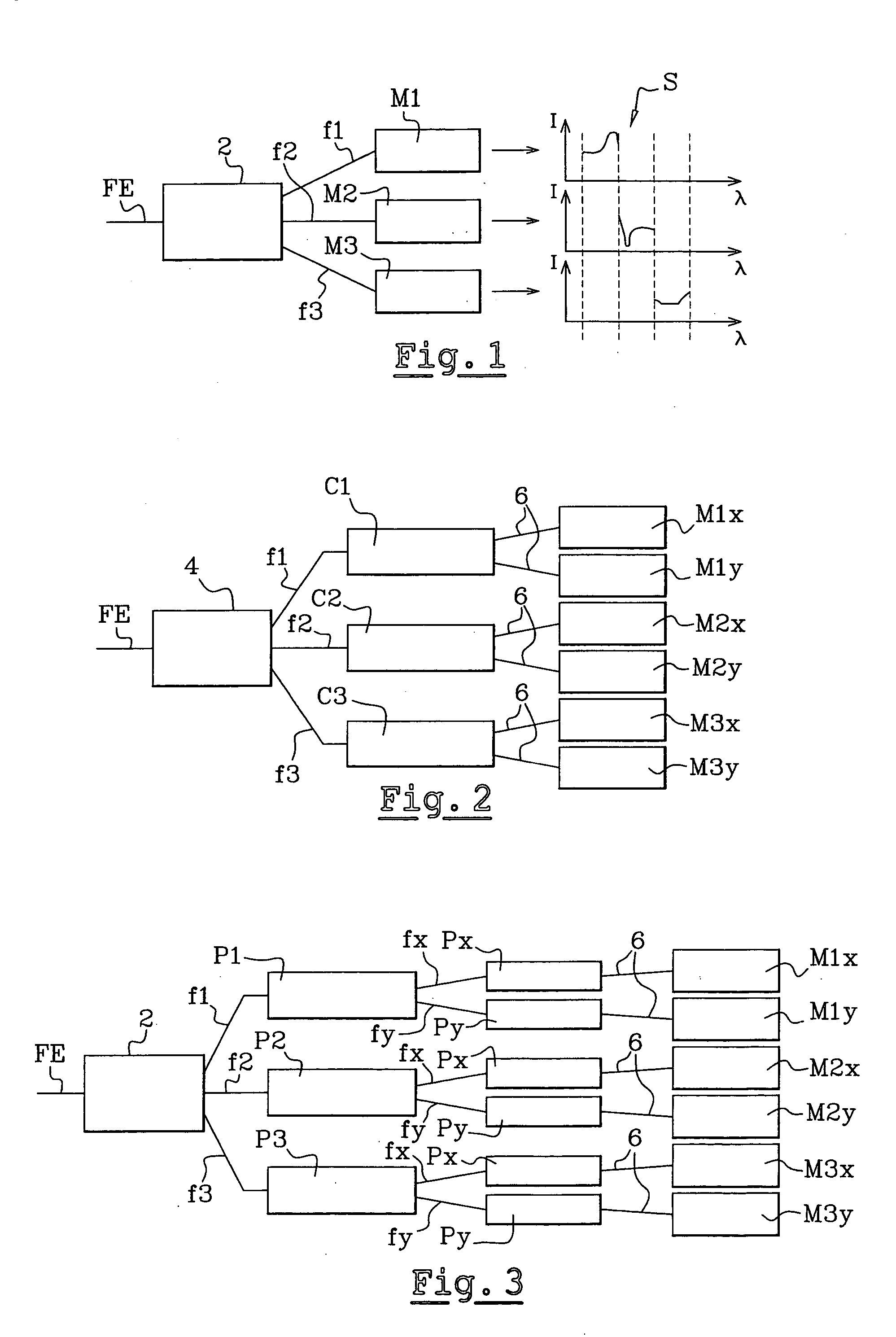
[0109] In the present invention, phasars are used for reasons of dispersion (the phasars having an elevated order of diffraction), compacity and diaphony performance. However, dimensioning calculations demonstrate that it is not easy to manufacture a single phasar for the entire wavelength range...


PUM


Abstract

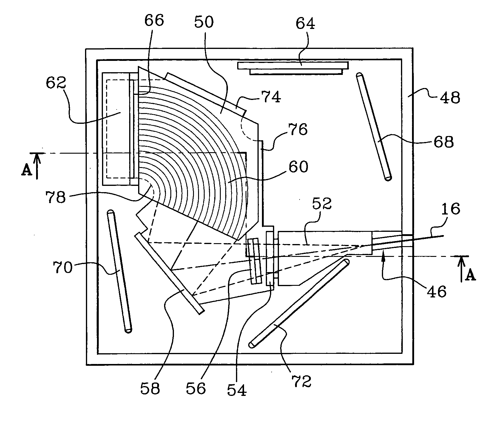
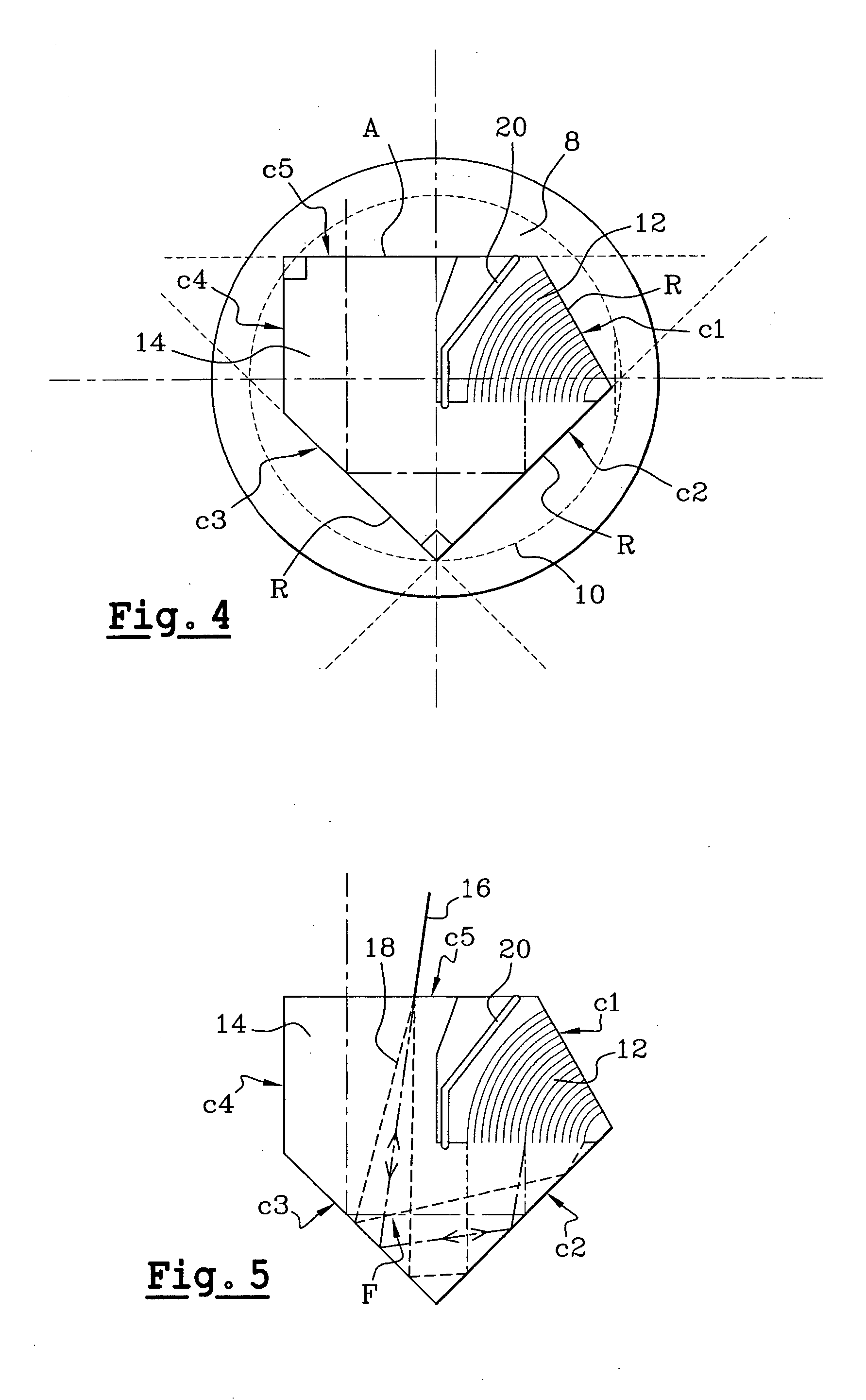
This spectrometer comprises at least one elementary spectrometer that comprises an optical phase array comprising a microguide assembly (12) and formed on a cleaved planar optical guide (14), reflecting means (24, 30, 32, 34) capable of successively reflecting radiation sent from the microguide assembly, for propagating this radiation in the folded form and in free space, means (26) for photodetecting the radiation so reflected and means (28) for focusing radiation on said photodetection means.

Description

[0001] The present invention relates to an optical spectrum analyzer also called "spectral analysis device" or, more simply, an "optical spectrometer."[0002] This spectrometer is particularly applied to infrared radiation in the field of high-speed optical telecommunications, for example. Other applications of the invention, in particular optical metrology, will be mentioned in the following.PRIOR ART[0003] Optical telecommunications has made possible a considerable increase in information rates by virtue of spectral and temporal coding. Currently, rates of the order of 40 gigabit per second are obtained on one single optical fiber. Thanks to DWDM or dense wavelength division multiplexing, the information rate exceeds 1 terabit per second.[0004] The increase in speeds that is necessary for establishing information transfer protocols (in particular on the Internet), requires a simultaneous growth in the spectral width of the telecommunications band and a reduction of the spectral int...

Claims


Application Information

Patent Timeline
IPC IPC(8): G01J3/18G01J3/02G01J3/28G01J3/36G02B6/34
CPCG01J3/02G01J3/0218G01J3/0256G02B6/1203G01J3/2803G02B6/12019G01J3/0291
Inventor BUGAUD, MICHELMAGNE, SYLVAINGRAND, GILLES
Owner COMMISSARIAT A LENERGIE ATOMIQUE ET AUX ENERGIES ALTERNATIVES
Learn More