Package substrate for electrolytic leadless plating and manufacturing method thereof

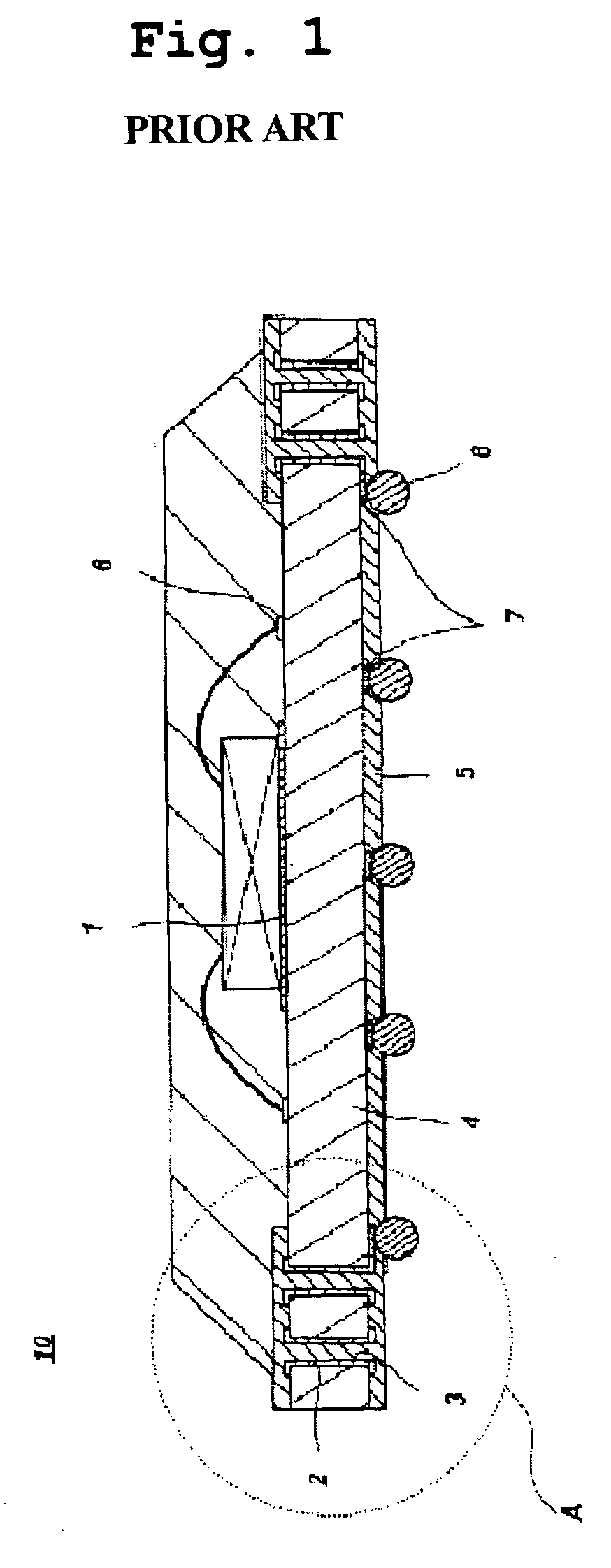
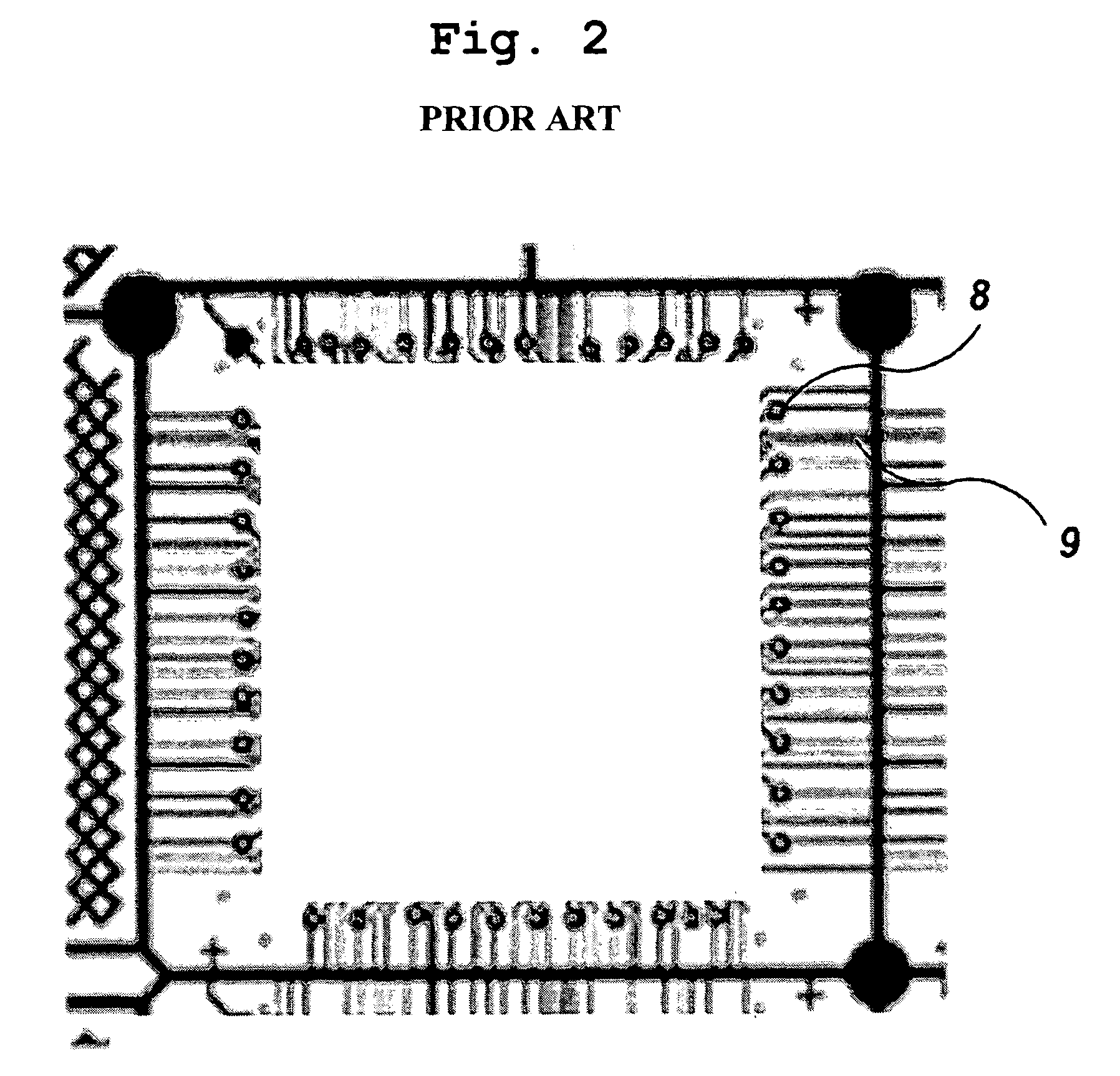
a technology of leadless plating and packaging substrate, which is applied in the direction of printed circuit aspects, conductive pattern reinforcement, printed element electric connection formation, etc., can solve the problems of weak pins or leads, easy breakage, and limitations on high-density circuit integration

Inactive Publication Date: 2004-08-05
SAMSUNG ELECTRO MECHANICS CO LTD
View PDF9 Cites 27 Cited by
  • Summary
  • Abstract
  • Description
  • Claims
  • Application Information

AI Technical Summary

Problems solved by technology

Although the PGA carrier has a large number of lead lines mounted on the small carrier, pins or leads are weak and thus are easily broken.
Further, limitations are imposed on high-density integration of the circuits.
Substantially, fabrication of high-density circuits is limited attributable to the lead lines.
However, in the conventional package substrate, due to highly dense circuits and miniaturization of a device using such circuits, a pitch (interval between the solder balls) of the solder balls 8 of the BGA package substrate 10 becomes excessively narrow.
Simultaneously, circuits around the bond finger 1 onto which the s

Method used


Image

  • Package substrate for electrolytic leadless plating and manufacturing method thereof
  • Package substrate for electrolytic leadless plating and manufacturing method thereof
  • Package substrate for electrolytic leadless plating and manufacturing method thereof

Examples


first embodiment

[0070] In the present invention, the wire bonding pad is subjected to electrolytic Au plating, and the solder ball pad is subjected to OSP metal finishing.

2.sup.nd EMBODIMENT

second embodiment

[0071] With reference to FIGS. 7a through 7c, there is sequentially illustrated a manufacturing process of the package substrate for electrolytic leadless plating according to the present invention.

[0072] In the present embodiment, the step of FIG. 7a is carried out after the steps of the above mentioned FIGS. 6a through 6l, and thus a description for the steps of FIGS. 6a through 6l is omitted.

[0073] After coating, exposing, developing and drying the solder resist 41, as seen in FIG. 6l, a dry film 43 as an electroless Au plating resist is coated, exposed and developed on the substrate, so that only the solder ball pad to be subjected to electroless Au plating is exposed (FIG. 7a).

[0074] Then, an electroless Au plated layer 44 is formed at a thickness of 0.03-0.25 .mu.m on the solder ball pad (FIG. 7b), after which the dry film 43 used as the plating resist is removed using a stripping solution (FIG. 7c).

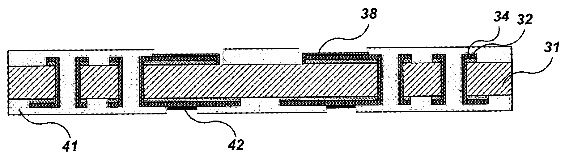
[0075] Comparing the first embodiment with the second embodiment, the solder b...

third embodiment

[0077] Turning to FIGS. 8a through 8m, there is sequentially illustrated a manufacturing process of the package substrate which is subjected to leadless plating according to the present invention.

[0078] In FIG. 8a, a plurality of through-holes 53 are defined in a base substrate as a copper clad laminate with layers 51 and 52. A surface of the base substrate and an inner wall of each through-hole are subjected to copper plating, to form a copper plated layer 54 (FIG. 8b). The Cu plating process is characterized by performing electroless Cu plating and then electrolytic Cu plating with respect to the base substrate and the inner walls of the through-holes.

[0079] Specifically, the package substrate comprises a multilayer sheet laminated with a plurality of copper clad laminates 51+52. The reference numeral 51 denotes an insulation layer and the reference numeral 52 denotes a copper foil laminated on a top surface of a bottom surface of the insulation layer 51. The CCL 51+52 has an inne...


PUM


Abstract

Disclosed is a package substrate for electrolytic leadless plating, characterized in that a wire bonding pad onto which a semiconductor chip is mounted is subjected to electrolytic leadless Au plating, and a solder ball pad is subjected to OSP metal finishing or electroless Au plating without use of plating lead lines, upon preparation thereof. A method of manufacturing the package substrate is also disclosed. The method includes Cu plating a whole surface of a base substrate having through-holes, developing a first dry film laminated onto the through-holes, removing a copper foil not covered with the first dry film, stripping the first dry film, exposing and developing a second dry film on the substrate so that only an upper portion to be subjected to electrolytic Au plating is exposed, grounding an electrolytic Au plating terminal to a solder ball pad, Ni-Au plating the wire bonding pad, removing the second dry film by a stripping solution, exposing and developing a third dry film, removing the exposed copper foil by an etching solution, removing the third dry film by a stripping solution, performing a series of processes of coating, exposing, developing and drying a solder resist, and subjecting the solder ball pad to OSP metal finishing.

Description

[0001] 1. Field of the Invention[0002] The present invention pertains, in general, to package substrates plated without the use of plating lead lines, and manufacturing methods thereof. More specifically, the present invention pertains to a package substrate for electrolytic leadless plating, in which electrolytic Au plating of the package substrate, such as substrate for ball grid array packages (BGA packages) or chip scale packages (CSP), is characterized in that when a semiconductor chip-mounted wire bonding pad and a solder ball pad are formed on the package substrate, the wire bonding pad is subjected to electrolytic leadless Au plating and the solder ball pad is subjected to OSP (Organic Solderability Preservatives) or electroless Au plating without lead lines for use in plating, and a method of manufacturing such a package substrate.[0003] 2. Description of the Prior Art[0004] Despite a streamlining trend in the IC (Integrated Circuits) field, for example, high integration, s...

Claims


Application Information

Patent Timeline
IPC IPC(8): H01L23/12H01L21/48H05K3/02H05K3/06H05K3/24H05K3/42
CPCH01L21/4846H01L21/4857H01L2924/01019H05K2203/1476H05K2203/1394H05K2203/0723H05K2203/072H05K2201/0352H05K3/427H05K3/426H05K3/243H01L2224/32225H01L2224/48091H01L2224/48227H01L2224/73265H01L2924/01078H01L2924/01079H01L2924/15311H05K3/064H01L2924/00014H01L2924/00H05K3/02
Inventor LEE, JONG-JINKIM, TAE-GUI
Owner SAMSUNG ELECTRO MECHANICS CO LTD
Why Eureka
Try Eureka