Model pattern simulation of semiconductor wafer processing steps

Inactive Publication Date: 2004-09-16
ACCENT OPTICAL TECH
View PDF19 Cites 62 Cited by
  • Summary
  • Abstract
  • Description
  • Claims
  • Application Information

AI Technical Summary

Benefits of technology

0038] The accompanying drawings, which are incorporated into and form a part of the specification, illustrate one or more embodiments of the present invention and, together with the description, serve to explai

Problems solved by technology

However, while SEM metrology can resolve features below 0.1 microns, the process is costly, requires a high vacuum chamber, is relatively slow in operation and is difficult to automate.
Optical microscopes can be employed, but do not have the required resolving power for sub-micron structures.
Because these diffraction models are computationally intensive, standard regression techniques generally cannot currently be utilized without introducing errors due to the performance of the regression, but if the errors are small or tolerable, a regression approach can be used.
Inference tools typically cannot measure an unknown pattern, which is to say determine relevant CD or other parameters, without first utilizing some form of "hint".
A major problem in the analysis is supplying the correct hints.
Sets of model patterns are not very useful in themselves.
The simulation may be complex, and include factors such as CD, relevant pitches, focus, exposure, resist type, resist thickness, t

Method used


Image

  • Model pattern simulation of semiconductor wafer processing steps
  • Model pattern simulation of semiconductor wafer processing steps
  • Model pattern simulation of semiconductor wafer processing steps

Examples


Embodiment Construction

)

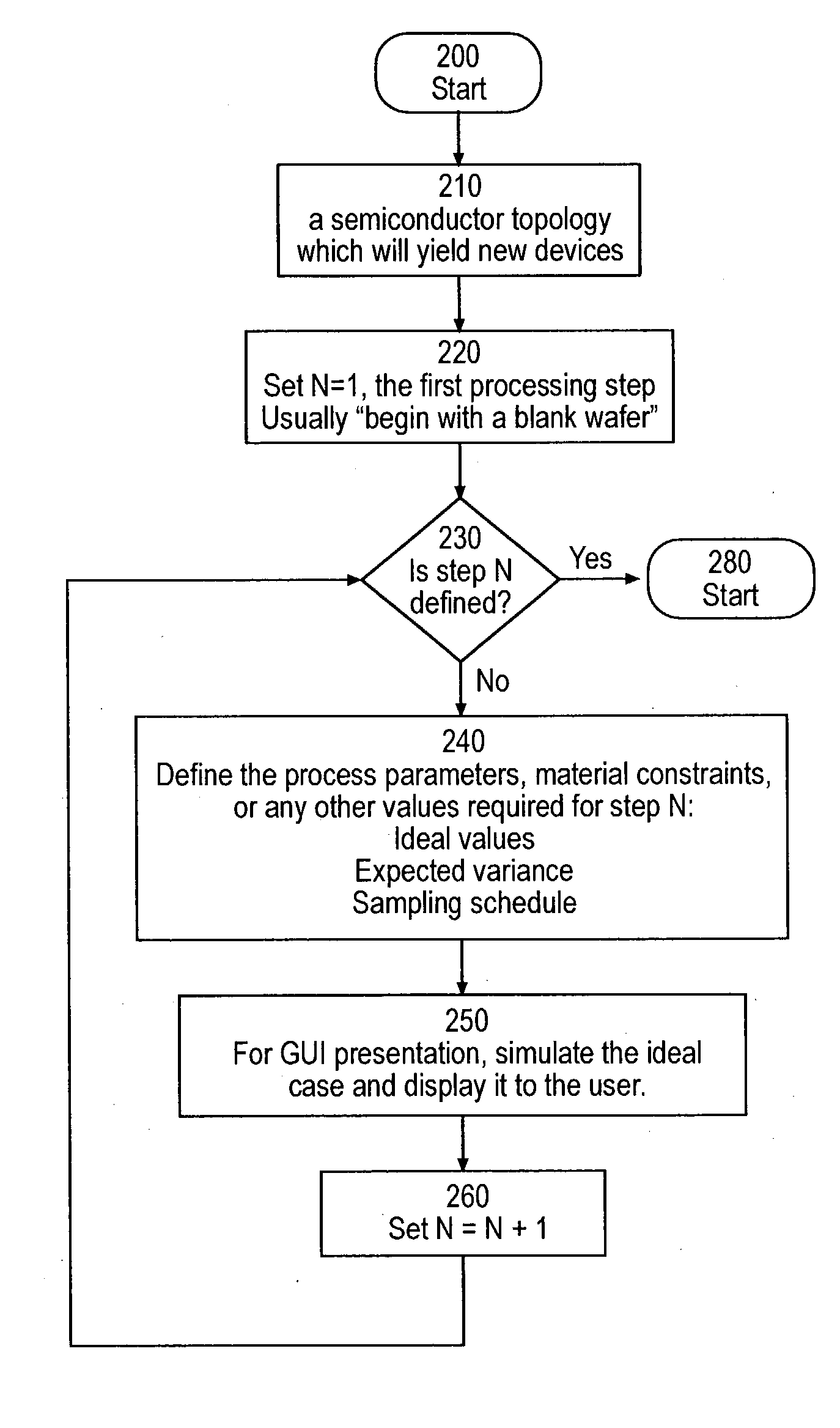
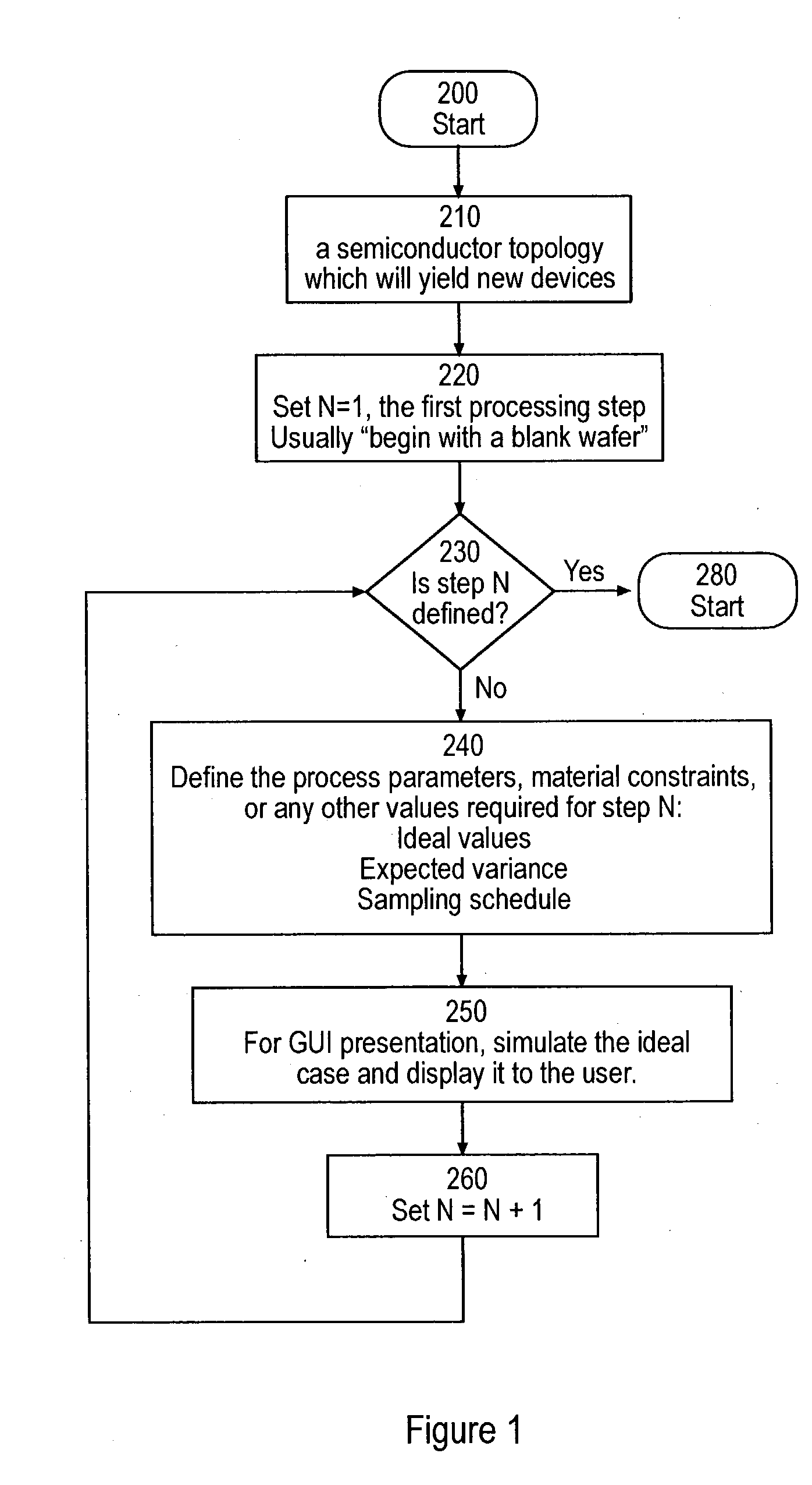
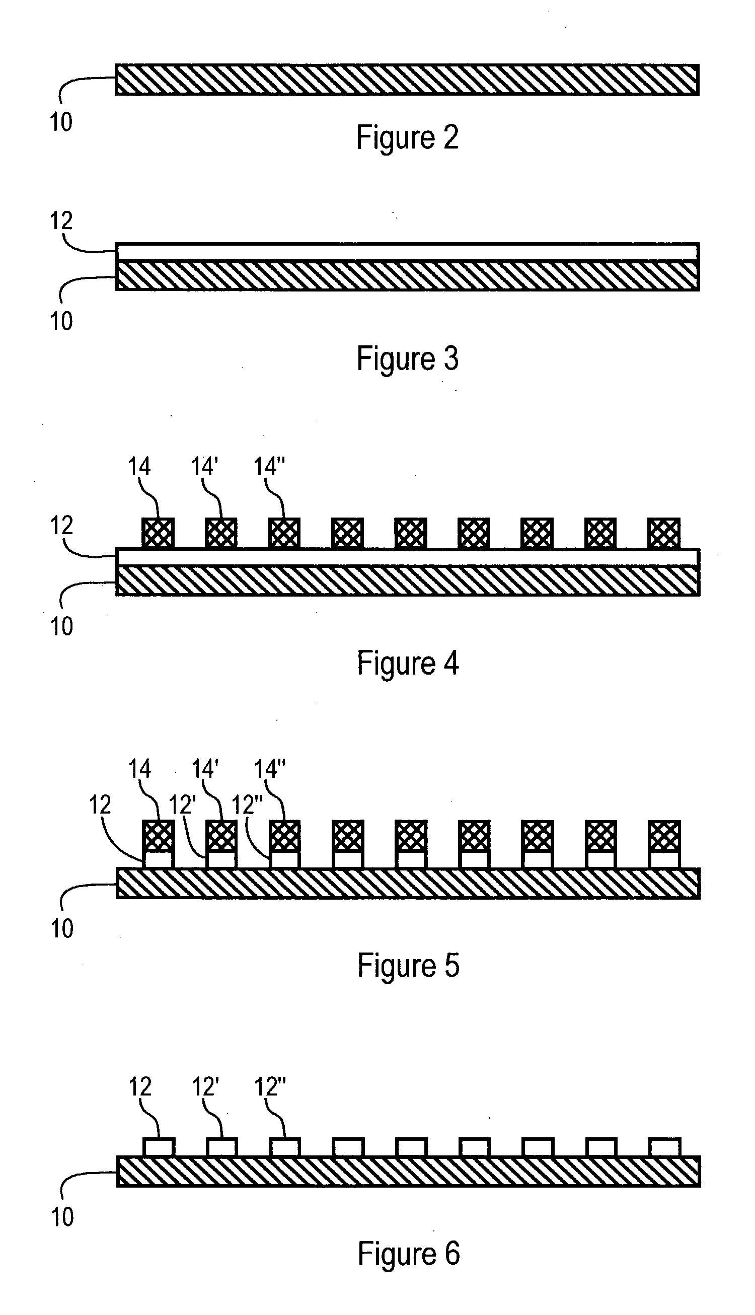
[0051] The invention provides systems and methods for generating model patterns and model pattern libraries together with derived model signals and model signal libraries, wherein the method of developing model patterns is based on the actual processes which a semiconductor wafer undergoes. These systems and methods present a number of advantages. In one embodiment, any pattern which can be produced can be modeled, limited only by the process model. Thus the ability to "draft" or otherwise specify a completed pattern is not required. New model patterns are generated via adjustments similar to those of the actual wafer fabrication process. Patterns only need to be drawn for the lithography step. If the pattern is generated using current techniques, then fewer primitive shapes are required. In general, lithography pattern data necessarily exists, and is required for the lithography mask. The mask data can be used in a process of automatically generating the pattern. Process engineers...


PUM


Abstract

Methods and computer program for determining a model pattern of a diffracting structure for use in semiconductor metrology, in which methods a series of process steps to be employed in fabrication of a diffracting structure, such as a diffracting structure fabricated on a semiconductor substrate employing a lithographic process, are specified, and each such specified process step is successively simulated to produce a model pattern of the diffracting structure. The methods further provides for generation of libraries of model patterns and simulated diffraction signatures based thereon, and optionally further provides for comparing diffraction signatures of measured diffracting structures to simulated diffraction signatures of members of the set of model patterns of the diffracting structure, selection of one or more close match simulated diffraction signatures, and deriving one or more parameters associated with the measured diffracting structures.

Description

[0001] 1. Field of the Invention (Technical Field)[0002] The present invention relates to metrology and process control in semiconductor manufacturing, and more particular to model patterns generated by simulation of semiconductor wafer processing steps and derivative libraries based thereon for use in radiation-based metrology, such as of lithographic or etch steps.[0003] 2. Background Art[0004] Note that the following discussion refers to a number of publications by author(s) and year of publication, and that due to recent publication dates certain publications are not to be considered as prior art vis-a-vis the present invention. Discussion of such publications herein is given for more complete background and is not to be construed as an admission that such publications are prior art for patentability determination purposes.[0005] Lithography is used to manufacture semiconductor devices, such as integrated circuits created on wafers, as well as flat-panel displays, disk heads and...

Claims


Application Information

Patent Timeline
IPC IPC(8): G03F7/20G06F17/50H01L
CPCG03F7/70625G03F7/705
Inventor KRUKAR, RICHARD H.
Owner ACCENT OPTICAL TECH
Why Eureka
Try Eureka