Method of manufacturing display device

a display device and manufacturing method technology, applied in the manufacture of electrode systems, electric discharge tubes/lamps, instruments, etc., can solve the problems of deteriorating production yield, high production cost, and limited regions of tft array substrates on the substrate of tft arrays

Inactive Publication Date: 2004-12-16
SEMICON ENERGY LAB CO LTD
View PDF66 Cites 59 Cited by
  • Summary
  • Abstract
  • Description
  • Claims
  • Application Information

AI Technical Summary

Problems solved by technology

However, a problem develops in that a production yield gets deteriorated and a production cost becomes higher with the increase in the scales of the display devices.
However, regions on the TFT array substrate in which the TFT is formed are very limited and almost all the resulting film is etched away.
Such an unnecessary material results in the factor that hinders the reduction of the raw material cost.
A large scale manufacturing apparatus for producing a large scale display device invites the increase in a cost of equipment with the increase in the capacity of a treating chamber, for example a vacuum apparatus having a greater exhaust capacity.

Method used


Image

  • Method of manufacturing display device
  • Method of manufacturing display device
  • Method of manufacturing display device

Examples


embodiment 2

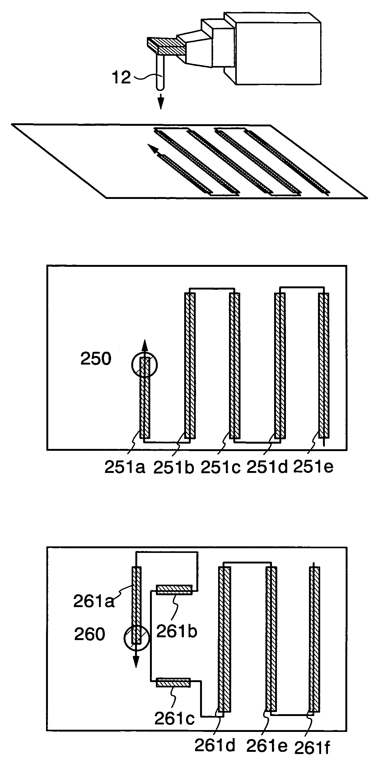
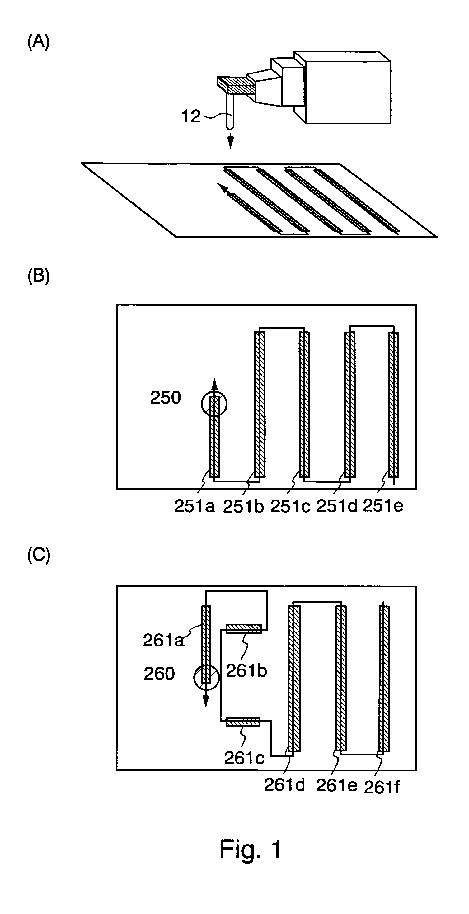
[0074] In this embodiment, a method of partially conducting plasma treatment such as etching, ashing, film formation, etc, by use of the apparatus shown in FIG. 6(A) to FIG. 7(D) will be explained.

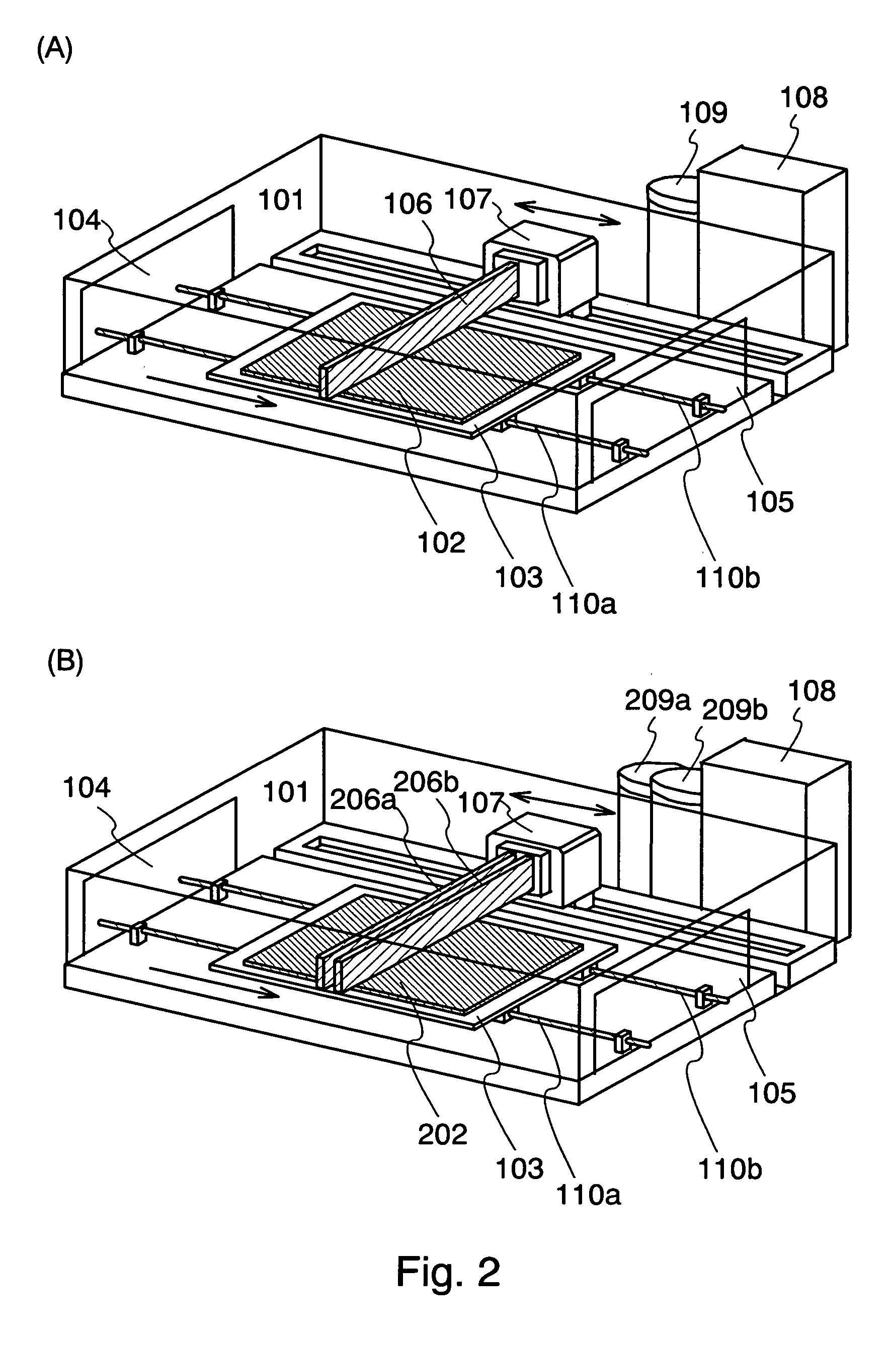
[0075] FIG. 6(A) is a top view of an example of the plasma treatment apparatus used in the present invention and FIG. 6(B) is a sectional view. In the drawings, a treated article 13 such as a glass substrate or a resin substrate typified by a plastic substrate each having a desired size is set to a cassette chamber 16. A conveying system of the treated article 13 includes horizontal conveying. When a substrate having a meter angle of the fifth generation et seq is used, however, vertical conveying that keeps the substrates under a longitudinal state may be employed to reduce an occupying area of a conveyor machine.

[0076] Inside a conveying chamber 17, the treated articles 13 arranged in the cassette chamber 16 are conveyed by a conveying mechanism (robot arm) 20 into a plasma treatment cha...

embodiment 3

[0087] In this embodiment, a method of partially forming a film under an atmospheric pressure or a pressure approximate to the atmospheric pressure by use of a method different from the method of the second embodiment will be explained with reference to FIG. 7(E).

[0088] In this embodiment, only the construction of the plasma generation means is different from that shown in FIGS. 6(A) and 6(B) and the partial film formation treatment is conducted by use of the same apparatus for the rest of portions. Therefore, only different portions from FIG. 7(A) that is an explanatory view of the plasma treatment means 12 shown in FIGS. 6(A) and 6(B) will be explained.

[0089] Unlike the plasma treatment means 12 shown in FIG. 7(A), this embodiment includes, inside a casing 36, film formation means in which the raw material is held in a pipe 37 passing through a filament 35 wound in a coil shape as shown in FIG. 7(E). The raw material heated by the filament 35 upon the supply of the current evapora...

embodiment 4

[0092] In this embodiment, a method of forming contact holes by forming a resist mask by using the liquid droplet jetting apparatus shown in the first embodiment and then conducting partial etching by the plasma treatment apparatus shown in the second embodiment will be explained with reference to FIGS. 8(A) to 8(C).

[0093] A plurality of resist films 51a to 51c is formed on the film 50 formed on the substrate by the method shown in the first embodiment (FIG. 8(A)). Incidentally, the film 50 in this embodiment is an insulating film of a silicon nitride film, a silicon oxide film, or the like and a plurality of gate wirings 58a to 58f formed of a conductor film and TFT connected thereto wirings are formed below the film 50.

[0094] Resist masks 53a to 53c having a plurality of openings 52a to 52f are formed by exposure and development.

[0095] Next, the reactive gas is partially blown to an inside portion (portion encompassed by dotted line 55a) of the portion at which the resist mask 53a...


PUM

PropertyMeasurementUnit
pressureaaaaaaaaaa
atmospheric pressureaaaaaaaaaa
frequencyaaaaaaaaaa

Abstract

The present invention proposes a manufacturing method of a display device that accomplishes a lower production cost of a display device by using means for partially forming a resist film and means for partially forming a film and etching or ashing by plasma treatment at or near the atmospheric pressure. The manufacturing method of the display device according to the invention is characterized by including a step of partially forming a conductor film at or near the atmospheric pressure and forming wirings. Here, the wirings include all kinds of wirings such as connection wirings for sending signals from external input terminals to a pixel portion, wirings for connecting thin film transistors (TFT) to pixel electrodes, and so forth, besides wirings operating as gate wirings and source wirings at the pixel portion of an active matrix type display device.

Description

[0001] 1. Technical Field[0002] This invention relates to a manufacturing method of a display device. More particularly, the invention relates to a manufacturing method of a display device that makes contrivances to a manufacturing method of transistors for driving a display device.[0003] 2. Background Art[0004] Scales of display devices such as a liquid crystal display device and an electroluminescence display device have become greater and greater. However, a problem develops in that a production yield gets deteriorated and a production cost becomes higher with the increase in the scales of the display devices.[0005] A TFT array substrate (TFT: Thin Film Transistors) that has been conventionally used for driving the display device is fabricated by repeating the steps of forming a film on an entire surface of a substrate, forming a resist mask by photolithography and etching and removing unnecessary portions of the film formed by use of this mask (refer to Patent JP-A-60202153, for...

Claims


Application Information

Patent Timeline
Patent Type & Authority Applications(United States)
IPC IPC(8): G02F1/1362H01L21/285H01L21/336H01L21/768H01L29/786H01L51/00H01L51/40
CPCG02F2001/136295H01L21/2855H01L21/28556H01L21/76802H01L21/76838H01L51/0023H01L29/66765H01L29/78669H01L51/0017H01L51/0019H01L51/0022H01L27/1292G02F1/136295H10K71/231H10K71/236H10K71/611H10K71/621
Inventor YAMAZAKI, SHUNPEI
Owner SEMICON ENERGY LAB CO LTD
Why Eureka
Try Eureka